A new microelectronics paradigm
In 2018, SkyWater began charting a new course for the industry through work to establish the world’s first carbon nanotube-based microelectronics architecture available with a PDK enabled design flow at a commercial foundry. This work is made possible through collaboration with MIT and the $61M 3DSoC program funded by DARPA, the largest awarded program in the first round of the ELECTRONICS RESURGENCE INITIATIVE (ERI).
About the Carbon Nanotube SoC Architecture
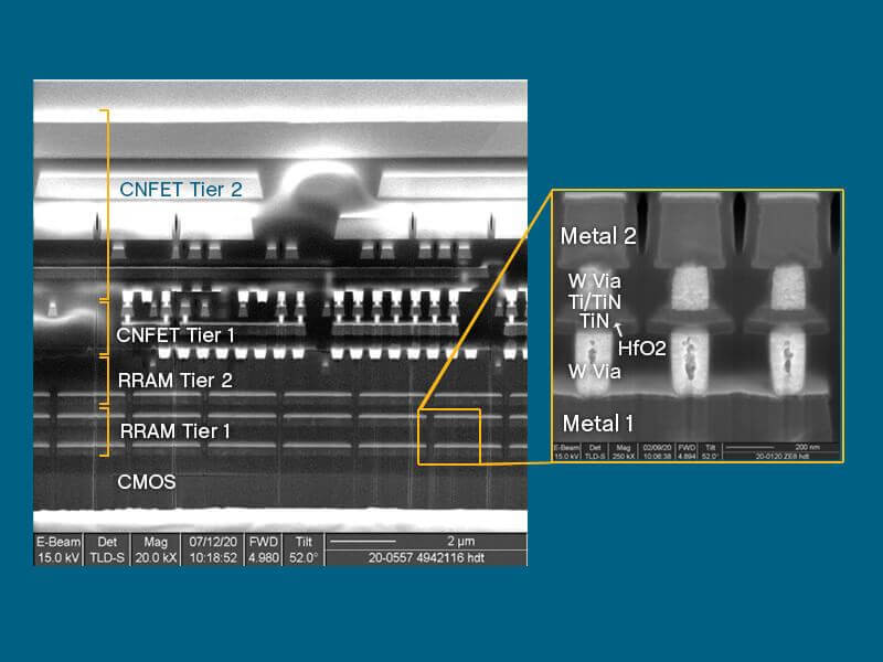
Conventional computing architectures consist of separate chips for processing/computing and memory. These chips are connected through physical interconnects which limit system performance. Through monolithic fabrication, 3DSoC will transform this system into a single integrated stack with multiple layers of computing built directly on top of one another, interleaved with layers of memory. The result is up to 50x SoC performance benefits at power using 90 nm 3D technology compared 7 nm 2D technology.
(Source: DARPA. Microsystems Technology Office Broad Agency Announcement. No. HR001117S0056. Sept 2017.)
It’s more than a science project
Carbon nanotube SoCs are produced in a production CMOS fab…and have demonstrated real life usable SoC architectures
- 16bit RISC-V microprocessor
More information about the Carbon Nanotube SoCs
This video is of Professor Shulaker’s remarks at the 2019 DARPA ERI Summit in Detroit, MI. Professor Shulaker of MIT was PI of the 3DSoC program, which partnered with SkyWater to demonstrate the architecture in a commercial foundry environment.
Following are links to NATURE articles discussing the process integration and implementation of devices in the carbon nanotube SoC architecture.

A Day in the Life of a Cleanroom Technician