
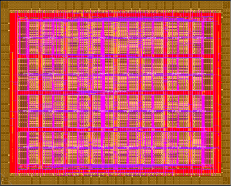
ASICs, SoCs &
CMOS + novel hybrid solutions
SkyWater’s proven CMOS technologies have enabled novel and disruptive products across demanding automotive, industrial, medical and defense markets for decades. As the production foundation, these technologies run in high volume and at world-class quality levels, as demonstrated by numerous quality-driven certifications. But it does not end there: SkyWater’s Advanced Technology Services enable the combination of standard CMOS platforms with a wide range of customer-driven additional devices to create highly customized, targeted integrated sensors, photonics, MEMS or other features.

90 nm and 130 nm process technologies
Billions of Devices Made for Automotive and Consumer Applications
- Infotainment, body electronics, ADAS/safety
- Wearables, smart home, personal electronics, vision systems, smart grid
- DNA sequencing, wireless interfaces, GPS receiver modules
- Read-Out ICs for thermal imaging applications
- CNT/3DSoC/ReRAM technology on 130nm for edge node processing and sensing
- SkyWater also has a state-of-the-art 90nm RadHard by Process technology

ThermaView℠ ROIC Solutions
- CMOS readout ICs for high responsivity infrared and sensor arrays.
- Reliable, stateside solutions for advancing thermal imaging technology in mission-critical and high-stakes applications.
- Low-noise, high-performance CMOS readout ICs designed to meet the demands of the aerospace, automotive, and industrial sectors.
SkyWater Design Partner Network
Our design partner network is a group of proven companies who are experienced with SkyWater’s manufacturing processes. Our partners ensure seamless collaboration to design and manufacture innovative semiconductors, fostering a robust ecosystem of expertise and innovation.
Meet our Design Partners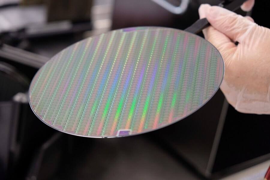
SkyWater MPW Shuttle Services
Most designs with volume potential will run on a multi-project wafer to verify performance and features prior to generating a dedicated mask set for production. Dedicated SkyWater MPW prototyping services are available on 130nm, 90nm, 90nm ROIC, and RH90.
- Prototype concepts with a fast feedback loop
- Verify IP and characterize device performance
- Regularly recurring shuttles

SkyWater Platform Data Sheets
SkyWater platforms include PDKs and other essential support — with your success in mind. Data sheets are available for the following platforms:
- S130
- S90
- S90LN
- RH90 (rad-hard platform for A&D applications)
Robust and flexible platforms for conventional and hybrid solutions
Production Process Flow Features
CMOS mixed-signal production process flows are the foundation of our technology offerings. These standard flows and custom variations enable innovators to bring novel ideas to market for silicon and next-wave technologies. Solutions can support conventional SoC and ASIC designs or be combined with your unique idea to create completely differentiated sensor, MEMS, photonics or other structures.
Scroll for More
| Technology | RH90* | S90/S90LN | S130 |
|---|---|---|---|
| Process | 90nm SOI | 90nm CMOS | 130nm CMOS |
| Wafer Size | 200mm | 200mm | 200mm |
| # Layers Metal and Composition | 1 – 5: Cu 6 & 7: Al | 7: Al | 5: Al |
| # Layers Local Interconnect | 0 | 2 Dual Damascene | 1 |
| Top Metal | 0.36 µm | 0.85 µm | 1.2 µm |
| Mask Steps | 34 – 36 | 28 – 38 | 30 – 34 |
| Temperature Range** (Qualified) | -55°C to +125°C Ambient | -55°C to +125°C Junction | -55°C to +125°C Ambient |
| ROIC (Focused Process Option) | No | Yes | No |
| ROIC Die Stitching | No | Yes | No |
| Planarized Viatop | No | Yes | No |
| Cryo Models** (Characterized) | No | 77K to 150K | No |
| Isolation | STI | STI | STI |
| Gate | Co-silicide Poly | W-clad Poly | Poly |
| Core Voltage | 1.2V | 1.2V | 1.8V |
| IO Voltage | 1.8V, 2.5V, 3.3V | 1.8V, 2.5V, 3.3V | 3.3V, 5.0V |
| High Voltage | No | No | 20+V, Drain-Extended CMOS (16V) |
| Multiple Vt Options | Yes | Yes | Yes |
| MiM Capacitor | Yes | Yes | Yes |
| Precision Resistor | 195Ω/□ (P-poly) | 120Ω/□ (N+ diff) | 2000Ω/□ 300Ω/□ (Both P-poly) |
| Inductor | No | No | No |
| OTP | In development | No | No |
| Polyimide | No | Yes – Cannot use with viatop | Yes |
| Substrates | FD SOI | 4 µm EPI | Bulk |
*RH90 is an ITAR restricted technology.
**Operating lifetime depends on operational profile.
Open-Source 130 nm CMOS Resources
SkyWater has partnered with Google to create the first open source process design kit, called SKY130, based on our 130 nm CMOS platform. Learn more about the PDK and opportunities to tapeout chips on open-source tool chains.

Open source SKY130 PDK on Github
Github hosts the SKY130 Open Source PDK. There you can find key information, links to resources needed to get started quickly, and support. The SKY130 PDK is supported by a dedicated and talented group who are equally excited by the opportunity of making chip development available to everyone.


Custom, Device-Ready Chips from SkyWater’s Design Partner Network