We’re building the next generation of heterogenous integration technologies
As our customers furiously innovate new ideas, we’re committed to enabling new architectures with the future of heterogenous integration technologies along with them. We are focused on building our technology portfolio around three categories we believe are the future of 2.5D and 3D architectures.
Silicon interposers
Bringing together high-density BEOL routing with through-silicon via electrical interconnects, SkyWater silicon interposers provide an advanced integration platform for combining multiple devices or chiplets in a highly compact form factor with power efficiency and improved functionality.
- All-copper TSVs (10um × 100um)
- Multi-layer routing at 1um line/space
- Support for bridge interposer devices (without TSVs)
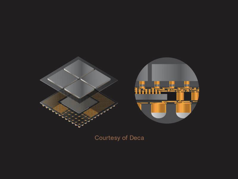
Fan-out wafer level packaging
SkyWater and Deca are establishing the first high-volume FOWLP capability in the U.S. to bring proven solutions for single and multi-die packaging and advanced heterogeneous integration capability for chiplets through 2.5D and 3D implementations.
- Integration of multiple dies in a package
- Deca Adaptive Patterning® Technology for high-yield routing
- Gen 2 technology will include finer line/space RDL and device I/O pitch capabilities
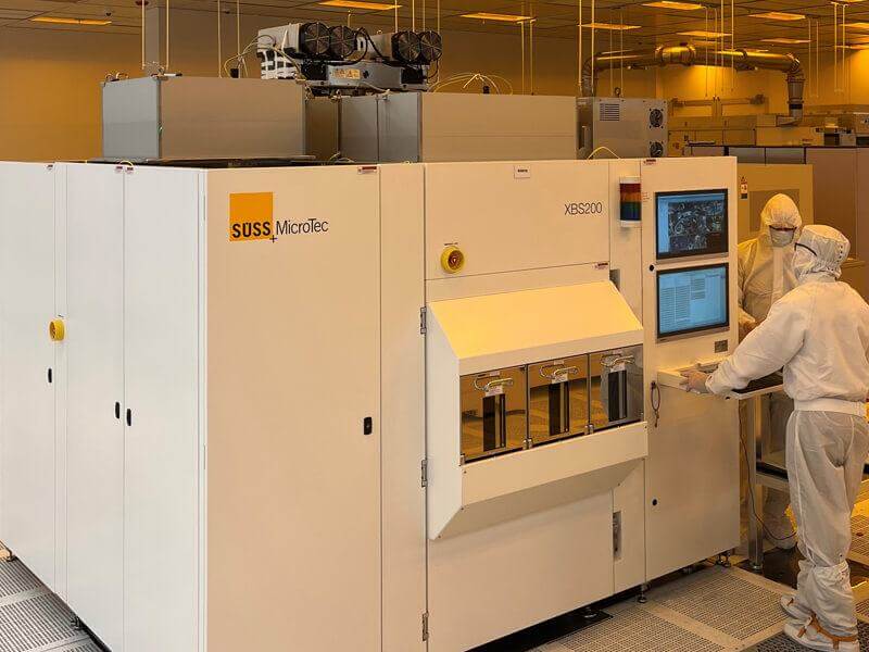
Wafer bonding
Wafer-wafer bonding allows the direct interconnection of one device to another through extremely short interconnects, resulting in lower power consumption, higher bandwidth and extremely compact device size. SkyWater is partnering with Adeia (Xperi) to offer ZiBond® and DBI® wafer bonding technologies, enabling extremely high interconnect density capability.
- Fine pitch interconnect at low temperature
- Strong mechanical bonding for dissimilar CTE materials
- Dielectric bonding with Cu electrical interconnects

Re-shoring Heterogeneous Integration Technologies