Forecast: 90 with Clear Visibility
by SenseICs Corporation
Trusted microelectronics design partner SenseICs developed its patented HDR ROIC for infrared imaging using SkyWater’s 90 nm technology — so you can see what’s coming…
Within the SkyWater Design Partner Network, SenseICs Corporation leverages their vast experience in designing advanced image sensor applications to blend seamlessly with SkyWater’s S90LN Low Noise ROIC-optimized platform. Recently awarded patents (US 11,570,392 and 11,770,635) for its High Dynamic Range Read Out IC using SkyWater’s 90 nm technology, SenseICs — our Columbus, Ohio-based design partner — is a solutions provider of thermal imaging and low size, weight and power, or SWaP high-performance microelectronics.
Today we’re turning our blog over to SenseICs so that we can look at some recent advancements in imaging technology and how you can work with them on your next project.
ROIC that offers 10 million electron capacity
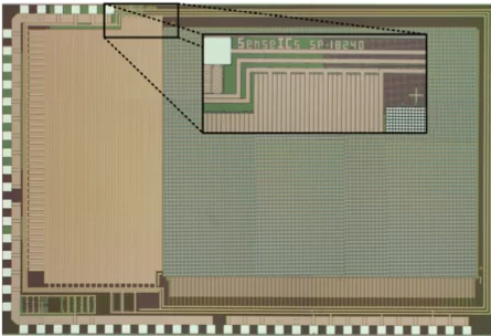
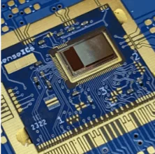
SenseICs’ HDR ROIC prototype showcases a full-well capacity of 10 million electrons — with less than 200 electrons of input referred noise. This intelligent digital HDR ROIC captures a lookahead coarse digital image (low resolution lookahead image shown) — facilitating frame-based event detection, smart windowing, context-adaptive sensing and compressive imaging.
Currently, SenseICs is collaborating with camera system partners to bring our HDR ROIC to market for MWIR and SWIR sensors. This technology operates at lower power and requires less data bandwidth.
Efforts are also underway to expand capabilities for a new event-based IR ROIC compatible with neuromorphic image processing. This advancement will leverage SkyWater Florida’s hybrid wafer bonding technology for 3D wafer stacking integration of next-generation IR sensors.
Pixel-level advanced imaging offers optimal visibility
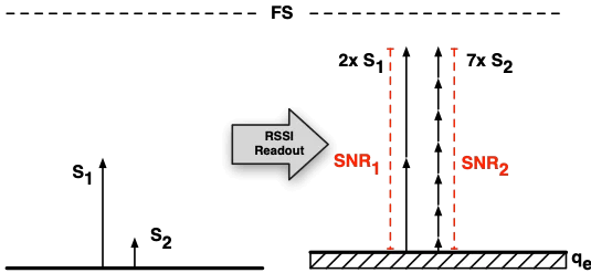
Optimal visibility — especially in challenging conditions — is essential. That’s why SenseICs advanced imaging sensors enable systems to capture images without compromising quality at either end of the light spectrum. The sensors work at the pixel-level to adapt and react to different levels of light — efficiently within one frame.
Leverage our deep experience with microelectronics for high-radiation environments
 Extreme environments, such as high-energy physics experiments or space, demand specialized, high-quality circuit solutions. SenseICs’ extensive experience in high radiation environments helps mitigate the negative effects throughout the design, testing and validation phases. Building on this expertise, SenseICs integrated circuits are designed with a focus on reliability and security. Key features include robust resistance to process variations, supply fluctuations and temperature extremes. We cover a broad spectrum from extreme radiation-hardened to radiation-tolerant applications. Our solutions range from multichannel radiation detectors, crucial for monitoring and measuring particle beams for particle physics, medical imaging and cancer treatment — to advanced long-range LiDAR ASICs featuring on-chip histogramming for NASA missions. These highly specialized chips not only enable new possibilities but also challenge the conventional performance limits of technology in high-radiation environments.
Rely on our IP Verified Core Technologies
 SenseICs’ proven success and verified intellectual property, or IP, has earned the trust of principal customers who are government agencies and prime contractors — including the Army Research Lab, Air Force Research Lab, Office of Naval Research, NASA, Thomas Jefferson National Accelerator Facility, KBR, Riverside Research, and Battelle.
IC trust is important in the design, production and life cycle of commercial and government systems. Through Verification and Validation, or V & V, SenseICs ensures that ICs fulfill their intended purpose while adhering to the highest security standards. These include the implementation of encryption cores, authenticity fingerprints, and comprehensive countermeasures designed to prevent information leakage. Our commitment to these principles guarantees that SenseICs’ technologies remain at the forefront of security and reliability, providing our clients with the assurance they need to operate effectively in their respective fields.
SkyWater’s multi-facility Trusted accreditations, aerospace & defense certification plus certifications in the medical and automotive industries means your project’s quality standards will be met — with certified and Trusted infrastructure.
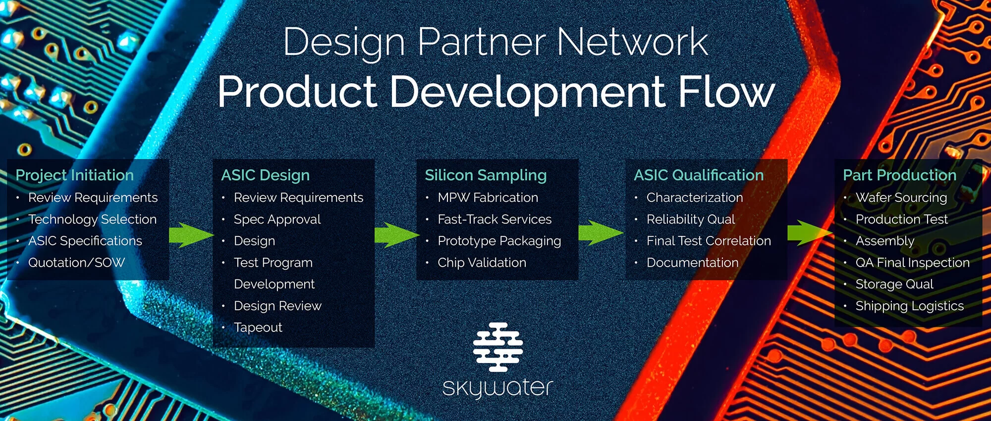
We offer many services within the SkyWater Design Partner Network as full turnkey solutions:
SenseICs will take you through the intricate journey of creating a microchip full turnkey solution, from conceptualization to the final stages of manufacturing and testing. Our multifaceted process flow is designed to ensure that the final product not only meets — but exceeds — the rigorous demands of modern technology applications.
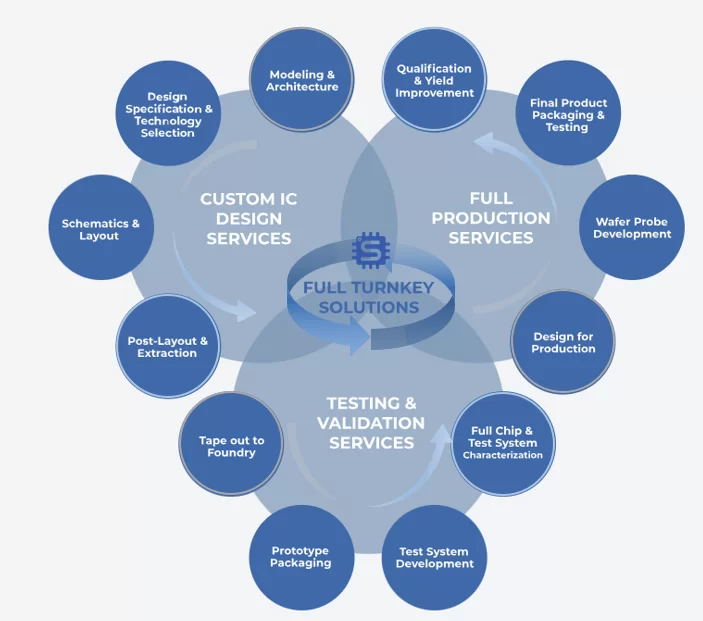
- Modeling & Architecture: Behavioral model of chip performance in overall system context
- Design Specification & Technology Selection: Specify design performance target specification and select optimal technology node for prototyping and production
- Schematics & Layout: Design schematics and layouts of the chip in selected technology node
- Post-Layout & Extraction: Integrated circuit layouts and physical implementation elements translated back into the electrical circuit components it is intended to represent for additional simulations and verification
- Tape out to Foundry: Final design is sent to manufacturing at SkyWater for mask set and design fabrication
- Prototype Packaging: Chip prototype is packaged as a means of ensuring the packaging is durable and the chip is testable to meet the specified prototyping needs
- Test System Development: Test bench circuit boards and periphery products ensure the designed chip technology functions correctly and meets specifications
- Full Chip & Test System Characterization: Complete characterization of the chip and test system to conclude final chip specifications and design limitations as it applies to the overall system requirements
- Design & Tape out for Production: Design integrated circuits to be fabricated in a full-mask set run with production specific criteria like testability, yield, EM emissions, etc.
- Wafer Probe Development: Develop wafer probe tester to test individual chips at wafer level prepackaging
- Final Product Packaging & Testing: Final packaged product is tested for reassurance then sent out to qualification
- Qualification & Yield Improvement: Process parameters are adjusted, and final improvements are made to achieve optimal performance in future fabrication runs
At SenseICs, our people are our greatest strength…
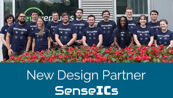
The SenseICs team is uniquely made up of leading-edge experts who come from diverse areas of engineering expertise. Because of our multidisciplinary nature, we approach design and development with a fresh perspective — which enables us to provide customers with innovative, yet proven, technology solutions.
At SenseICs we strive to create lasting partnerships within the government and commercial microelectronics industry. Capitalizing on relationships with academic institutions and research labs, we utilize a unique strategy of training and hiring engineers and other personnel through internships and post-graduate recruitment to find the latest talent.
Our cutting-edge technology, experience, and commitment to American innovation positions us well to achieve the goal of becoming a leading fabless semiconductor component provider to microelectronic system integrators.
Read more about our team including leadership bios:
https://senseics.com/about-us/

Ready to see more?
Connect with the Design Partner Network to get started.
We will assign a technologist to start the conversation. If you like what you hear and want to continue our journey together, just sign an NDA.
 One example of how we can engage with you through our design partner network is offering a long-term supply for legacy chips. Recently, a leading technology company reached out to SkyWater with a desire to leverage our domestic presence for long-term supply stability on several designs that needed to be turned quickly. This customer could not get the attention of their IDM given their volume profile. Partnering with IC Enable, the customer was able to secure a full domestic turnkey solution. The close working relationship between IC Enable and SkyWater made all the difference.