
QUANTUM SOLUTIONS
Quantum innovation doesn’t fit neatly into the traditional foundry model. SkyWater Quantum Solutions helps quantum hardware providers develop, integrate, and scale their technology — fast iteration, customized development, and flexible engagement.
Built Differently for Quantum
Our approach is built around the realities of quantum technology development, with the flexibility, capabilities, and partnership model to support what comes next.
-

From Breakthrough to Scale
Enabling quantum technology from R&D breakthrough to industrial scale.
-

Open & Neutral
Open. Neutral. Collaborative. Built for the whole ecosystem.
-

Full Stack Enablement
Flexible R&D prototyping, 200mm CMOS foundry, and advanced packaging all on U.S. soil.
-

Your Innovation Remains Yours
We industrialize the enabling technology, not your differentiation.

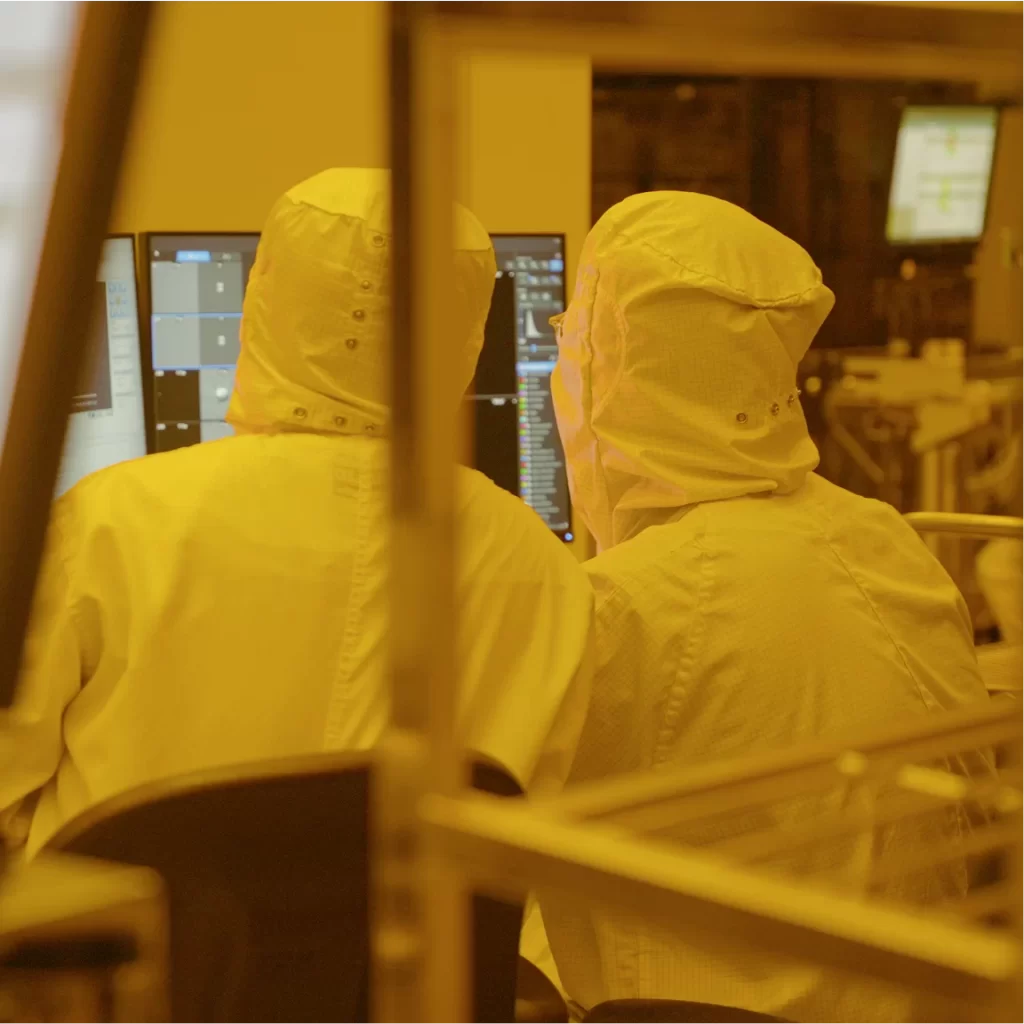

LAB TO LINE, WITHOUT LEAVING THE FAB
SkyWater supports quantum customers across the full technology lifecycle, from early proof of concept and rapid prototyping through customization, qualification and volume manufacturing.
Unlike conventional or specialty foundries, our flexible model combines development in leading user facilities with in-fab engineering expertise, modular process building blocks and a high tolerance for customization, helping customers iterate quickly without starting over. When a technology is ready to scale, it can transition seamlessly into production within the same foundry ecosystem, reducing requalification, accelerating time to market and supporting everything from priority low-volume runs to high-volume manufacturing and advanced packaging. Your technology is the differentiation; our role is to help industrialize it.
Your technology is the differentiation. Our role is to help you industrialize it.
Rapid prototyping for aggressive roadmaps
Relentlessly focused on wafer velocity: rapid iteration to meet the pace your roadmap requires.
Customize without starting over
Modular process building blocks and dedicated quantum solutions engineers who understand your device, not just your design file.
Move to volume, same fab
The technology foundry that gets you to first wafer also takes you to production — no requalification with a new vendor.
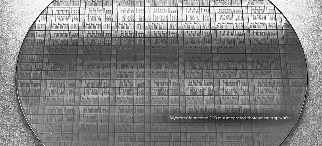
Two core platforms, backed by supporting technologies
Routing and controlling quantum signals sits on two core platforms — superconducting and photonics — with heterogeneous integration and advanced packaging as supporting technologies that extend both, backed by SkyWater’s DMEA-accredited, U.S.-based manufacturing.
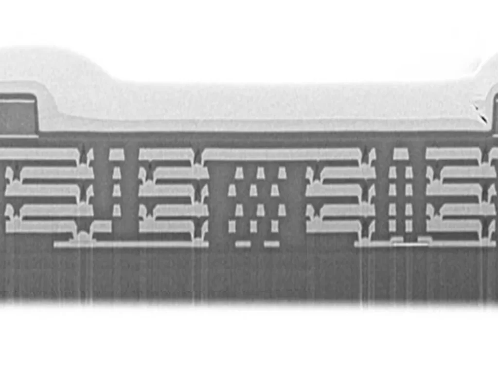
CORE PLATFORM: SUPERCONDUCTING ROUTING
SC250 · Superconducting Routing
High-density niobium interconnects for the cryogenic stack — a 6-layer niobium process as standard, with an integrated Josephson-junction layer for customized superconducting logic (SFQ).
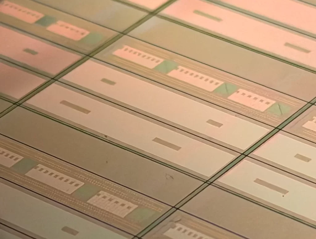
CORE PLATFORM: QUANTUM PHOTONICS
SP90 · Quantum Photonics
A low-loss silicon nitride platform spanning visible-to-near-IR (400-2+ um), with automated wafer characterization capabilities at wavelengths that matter for quantum.
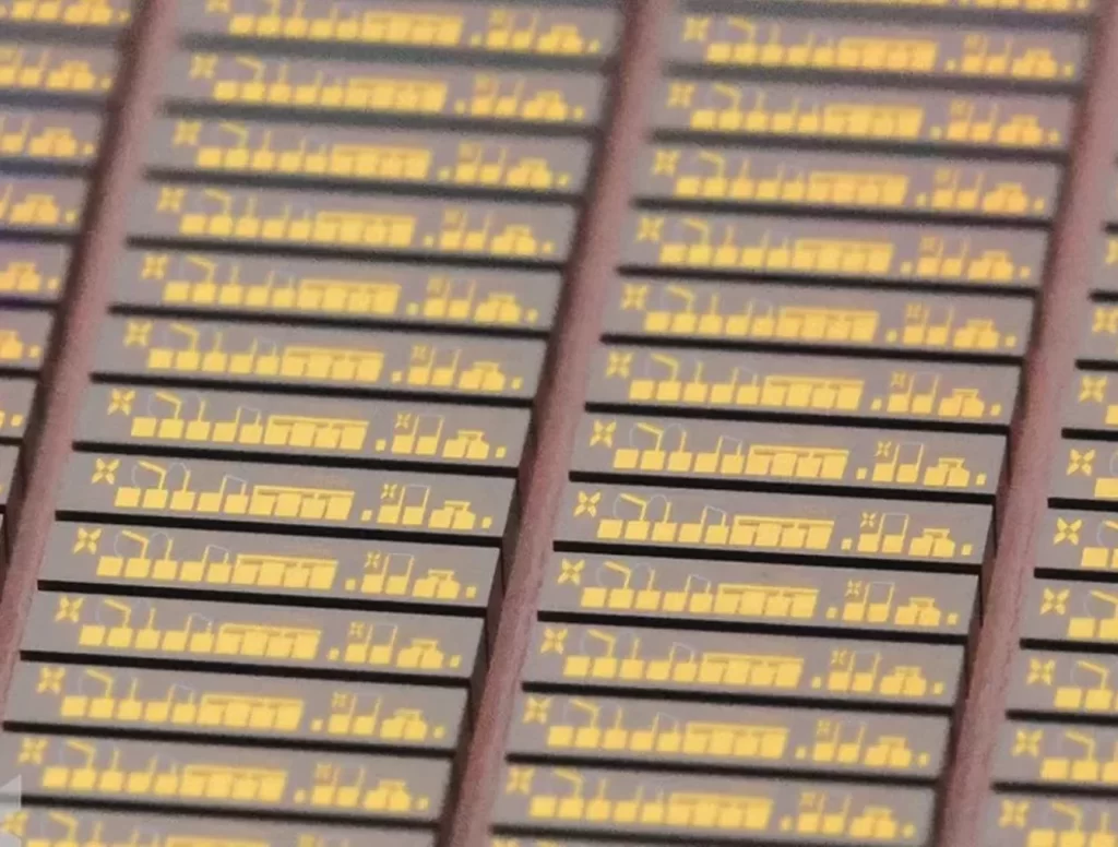
SUPPORTING TECHNOLOGY: NOVEL QUANTUM MATERIALS
Heterogeneous Integration
Beyond standard CMOS: diamond, thin-film lithium niobate, and III-V, heterogeneously integrated onto the SP90 platform.
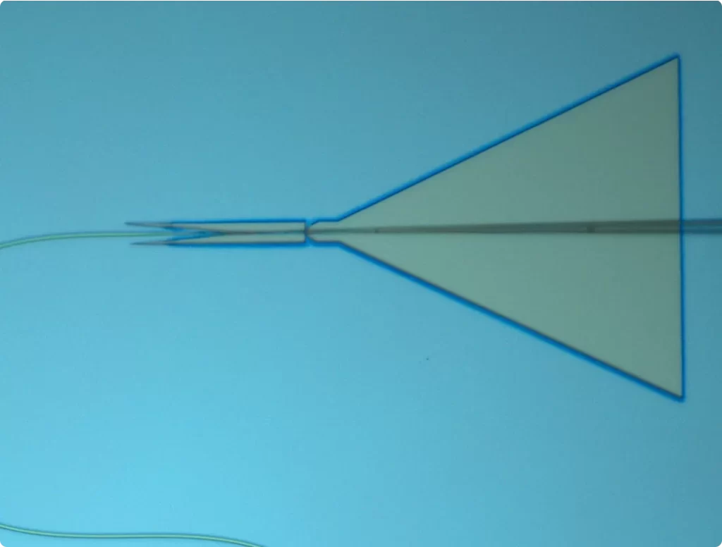
SUPPORTING TECHNOLOGY: ADVANCED PACKAGING
Advanced Packaging
2.5D/3D integration, interposers, wafer/die bonding, and fiber attach, including proprietary technology to achieve < 0.5 dB with cryogenic compatibility.
NEED TECHNOLOGY NOT COVERED ABOVE?
SkyWater Quantum Solutions can help – our business is designed to be flexible to your needs.
TRUSTED ECOSYSTEM PARTNER

-
 Learn More
“SkyWater brings deep semiconductor manufacturing expertise, advanced fabrication infrastructure, and process development capabilities, while QuamCore contributes innovations in superconducting digital circuit design, cryogenic measurement, and characterization. This type of close collaboration between U.S. manufacturing and deep-tech innovation is essential for enabling the next generation of quantum computing.”
-
 Learn More
“SkyWater brings an established track record of supporting quantum programs and gives us access today to the specialized capabilities needed to advance our Quantum System-in-Package. Combining SkyWater’s rapid, flexible development support with a repeatable commercial wafer services model gives us the manufacturing and cost visibility needed to iterate quickly and build a clear path toward commercial deployment.”
Prof. John Martinis, CTO & Co-founder of Qolab

REAL WAFERS, REAL PACKAGES, UNREAL SPEED
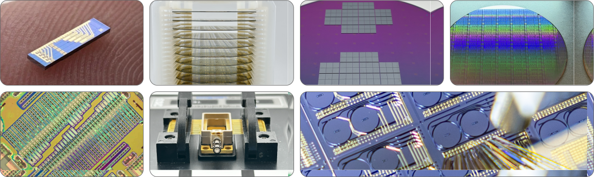

LET’S GET YOUR FIRST WAFER MOVING
Whether you’re developing quantum processors, cryogenic electronics, advanced packaging solutions, or emerging quantum technologies, SkyWater can help move your innovation from research to scalable manufacturing.