
SP90
Silicon Nitride Photonics
SP90 combines a low-loss SiN foundation on 200 mm silicon with advanced optical capabilities your system needs.
Building a photonics startup? Explore SkyWater OnRamp for a path to SP90.
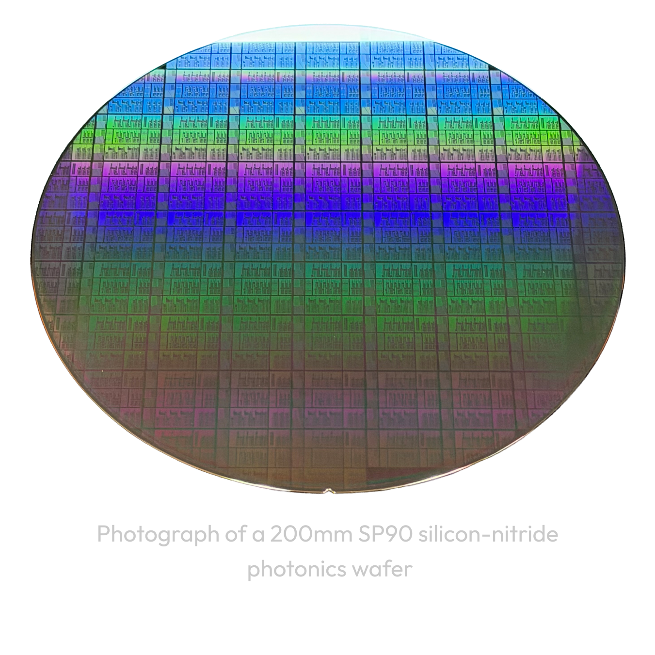
200 mm
silicon wafer platform
400–2000+ nm
supported optical wavelength range
Photonic integrated circuits designed for your needs
Quantum systems use different wavelengths and materials. SP90 starts with silicon nitride waveguides designed for visible-to-infrared operation, with thickness options for different optical bands. Multiple SiN layers add flexibility in photonic circuit design.
SP-CORE provides the photonic backbone. Heterogeneous integration and packaging capabilities extend it to enable light generation, modulation, optical interfaces, and photon detection on chip.
Customizable to support your application – quantum, sensing, communications, and much more.

Choose the capabilities
your circuit needs
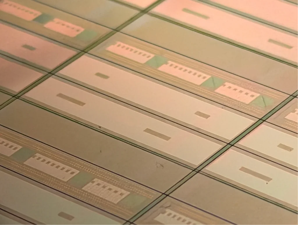
Select a technology’s name or schematic to explore its capabilities and device imagery.
SiN photonics on a shared 200 mm silicon foundation.





SP-CORE
Low-loss routing
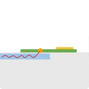
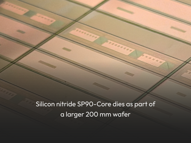
Low-loss SiN waveguides support visible-to-infrared routing, with thicknesses matched to the optical band and multiple SiN layers for flexible circuit design. Photonic building blocks include bends, splitters, crossings, rings, Mach–Zehnder interferometers, heaters and edge couplers.
Visible-to-infrared photonics
SP-PKG
Optical I/O
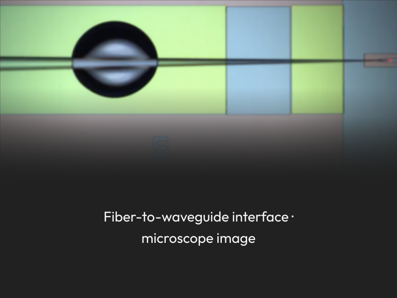
Tapered-fiber interfaces couple light between optical fibers and on-chip SiN waveguides. Optical coupling and packaging are tailored to the operating wavelength and temperature.
Fiber-to-chip interfaces
SP-LAS
Active III-V
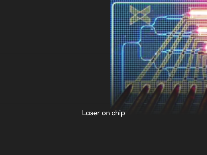
III-V materials add light generation, amplification, detection and modulation to SiN photonics.
III-V gain materials combine with SiN photonic cavities for on-chip light generation and amplification. Integrated monitor photodiodes provide optical power readout and modulators add data transfer and sideband generation.
Integrated light generation, amplification, detection and modulation
SP-DIA
Diamond integration
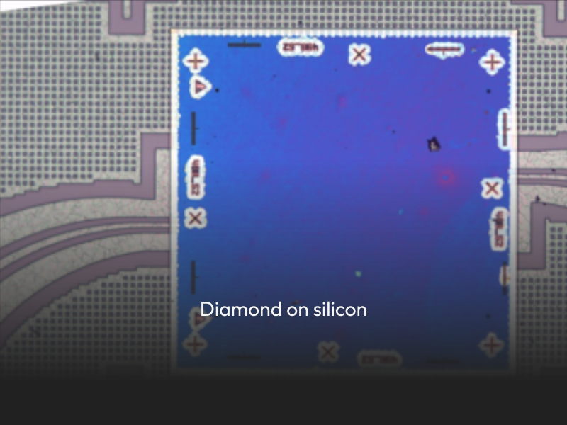
Bonded diamond membranes and optical transitions between SiN and diamond support quantum memory and sensing applications.
Diamond–SiN optical interfaces
SP-NBN
Photon counting
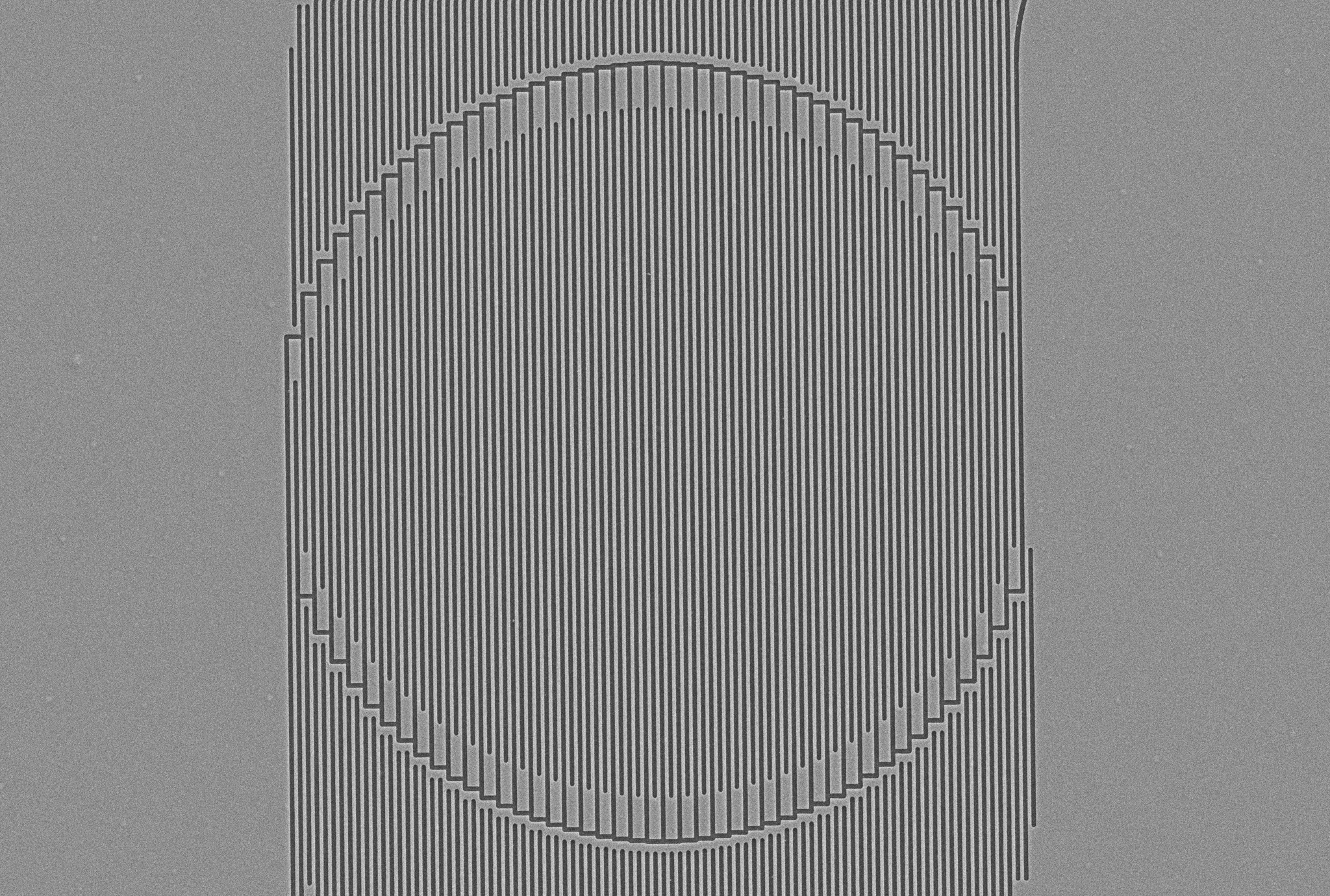
Superconducting niobium nitride nanowire single-photon detectors (SNSPDs) integrate with SiN waveguides for on-chip photon counting at cryogenic temperatures.
Waveguide-coupled single-photon detection
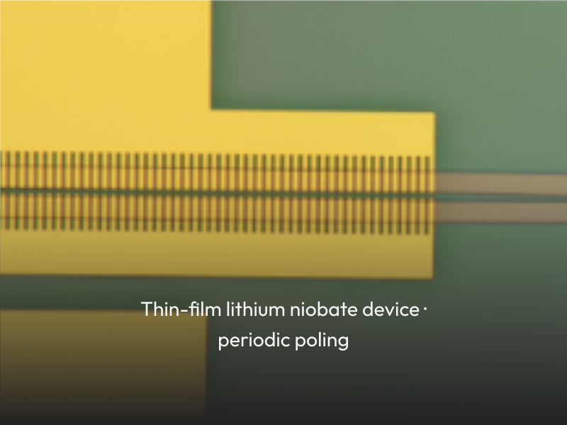
SP-NLO
Nonlinear optics
Thin-film lithium niobate enables nonlinear frequency conversion and electro-optic modulation, supporting optical links between device wavelengths and the telecom band.
Frequency conversion and electro-optic modulation
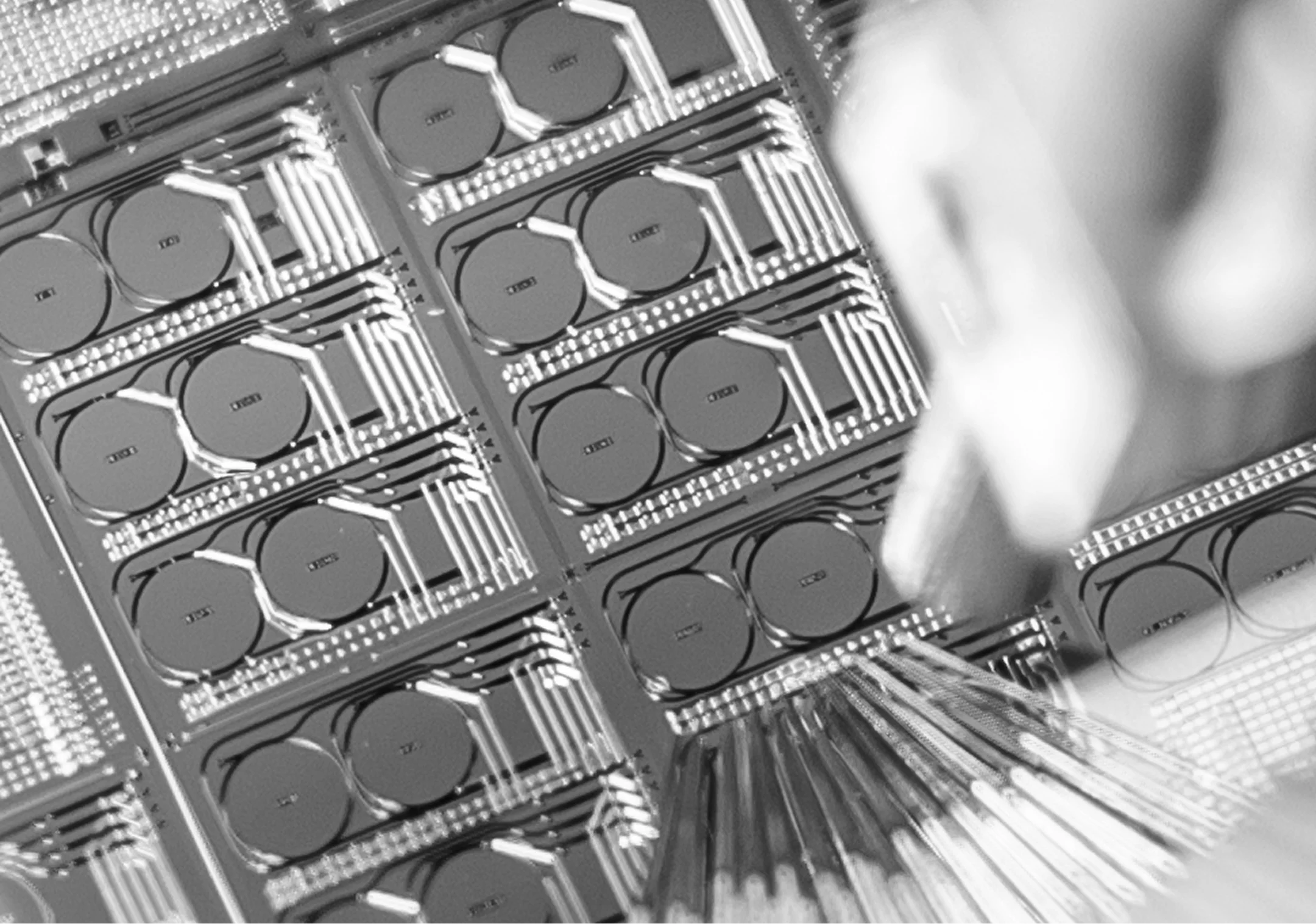

Wafer-level characterization
Measured across the wafer. More updates to come.
We’re mapping optical performance across 200 mm wafers at visible and infrared wavelengths. Initial results are available, with characterization and optimization continuing.
Building toward integrated systems
Illustrative combinations on the SP-CORE backbone. Each system requires its own integration and validation work.

-
Sensing
Integrate a laser source with on-chip amplification, power monitoring, and electronic control for NV magnetometry.
SP-LAS + SP-PKG
-
Optical networking
Connect quantum photonic devices to telecom fiber through wavelength conversion and optical packaging.
SP-NLO + SP-PKG
-
Photon detection
Develop a cryogenic, waveguide-coupled detector module with a fiber input and electrical readout.
SP-NBN + SP-PKG


A head start on your first wafer
OnRamp startups can access SkyWater professional engineering services to scope a foundry-validated roadmap to bring their innovations from lab to fab.
Selected OnRamp companies can also get early access to wafers through paid access to internal SP90 Prototype runs.
Your innovation remains yours. We help you manufacture it.
For other SP90 engagements, talk to our team.
EXPLORE SKYWATER QUANTUM SOLUTIONS
Quantum innovation doesn’t fit neatly into the traditional foundry model. SkyWater Quantum Solutions helps quantum hardware providers develop, integrate, and scale their technology through rapid iteration, customized development, and flexible engagement.