
SEMICONDUCTOR
FOUNDRY SOLUTIONS
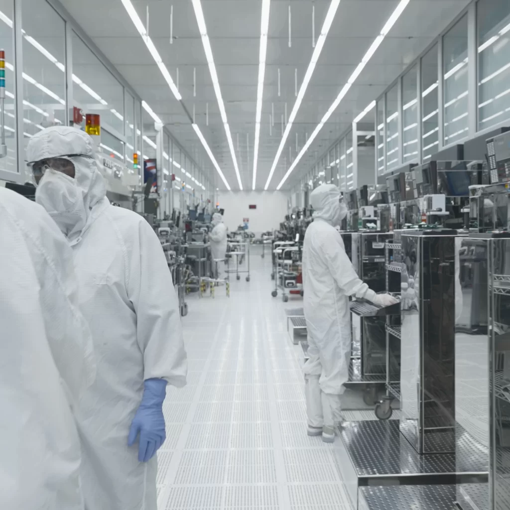
U.S.-based wafer manufacturing and advanced packaging for commercial and mission-critical applications. SkyWater combines production scale, automotive quality heritage and specialized engineering capabilities to support established products and emerging technologies.
U.S. MANUFACTURING. PROVEN AT SCALE.
SkyWater’s Minnesota and Texas wafer fabs combine high-volume production, domestic dual-sourcing capabilities and a longstanding automotive supply heritage.
-

520,000 wafers per year across two fabs
Combined annual wafer output supports high-volume consumer, automotive and industrial markets.
-

Domestic dual-sourcing capabilities
Minnesota and Texas support supply continuity through process alignment and qualification matched to each customer’s program.
-
Quality proven through automotive production
Years of automotive supply underpin our manufacturing discipline, from process qualification and reliability requirements to production control and consistent quality.
-

ITAR, Trusted and secure wafer processing supported.
SkyWater supports ITAR requirements, DMEA-Trusted Foundry services and secure wafer processing for sensitive commercial, aerospace and defense programs.

ADVANCED PACKAGING + INTEGRATION
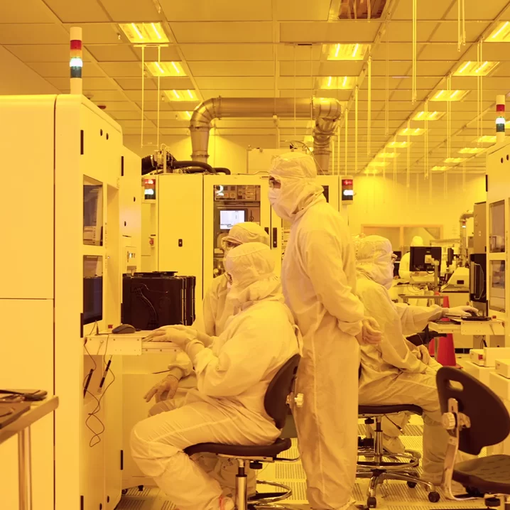
System performance increasingly depends on how devices connect. SkyWater’s advanced packaging offering brings together complementary technologies for semiconductor applications spanning computing, sensing, aerospace and defense.
Silicon interposers & chiplet integration
Dense routing and interconnects connect multiple devices in compact architectures.
Fan-out wafer-level packaging
Integration approaches support single- and multi-die systems with flexible package-level interconnects.
Wafer bonding & 3D integration
Compact device stacks enable high-density connections between complementary technologies.
Our Florida advanced packaging operation supports domestic integration capabilities, with process development, qualification and manufacturing plans aligned to customer requirements.
WAFER FAB TECHNOLOGIES +
CAPABILITIES
-

Mixed-Signal CMOS
Learn MoreEstablished platforms for ASICs, sensing, control and embedded applications, supported by PDKs, available IP and design partners.
-

Imaging & Readout ICs
Learn MoreProcess capabilities for infrared detectors and sensor arrays.
-

Radiation-Hardened Technologies
LEARN MORESpecialized microelectronics for radiation environments and demanding mission requirements.
-

MEMS & Custom Processes
LEARN MOREDevice and process integration for sensing and biomedical applications.
CONNECTED THROUGH TECHNOLOGY-AS-A-SERVICE
Our Technology as a Service model connects process engineering, wafer manufacturing and advanced packaging to support established products and new technologies.
STRENGTHENING THE U.S. MICROELECTRONICS SUPPLY CHAIN
SkyWater invests in domestic wafer manufacturing and advanced packaging capabilities—and advocates for trade policy and federal procurement reform that strengthen U.S. microelectronics supply-chain participants.
Our commitment connects production capacity, technical expertise and policy leadership to support a competitive domestic industry.

LET’S DISCUSS YOUR NEXT PROGRAM
Connect with our team about wafer manufacturing, advanced packaging or the development work needed to bring your product to production.