
Thermaview ROIC Solutions
SkyWater’s ThermaView™ 90nm CMOS solution provides the performance and reliability needed to support advanced thermal imaging systems across demanding commercial, industrial, aerospace, and defense applications. Whether supporting emerging sensor architectures or established infrared technologies, ThermaView combines CMOS design expertise with U.S.-based manufacturing capabilities to help customers develop differentiated imaging solutions.

Engineered for Performance
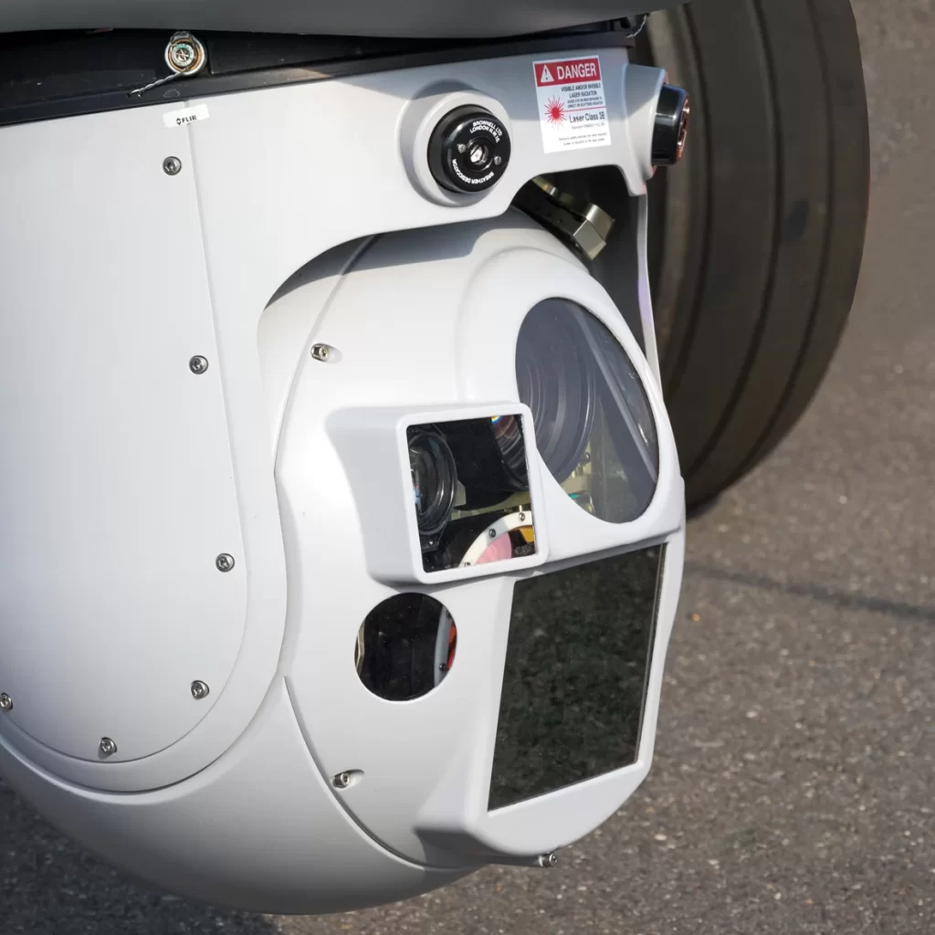
ThermaView provides the foundation for readout integrated circuit (ROIC) products. A ROIC serves as the electronic interface between a detector or focal plane array and the broader imaging system. In thermal imaging systems, ROIC performance directly influences sensitivity, image quality, speed, power consumption, and overall system capability.
ThermaView Advantages:
- Low Noise Performance
Designed to maximize image quality and support highly sensitive infrared detection. - High Responsivity
Optimized architectures support accurate signal acquisition across infrared detector technologies. - CMOS-Based Reliability
Leverages mature CMOS manufacturing processes for consistent performance and scalability. - Application Flexibility
Supports a range of detector formats, architectures, and mission requirements.

Manufacturing Capabilities
- 200 mm wafers
- 90 nm CMOS, 7 metal layers
- 1.2 V core; 1.8 V, 2.5 V and 3.3 V IO
- Qualified temperature range: -55°C to 125°C
- Characterized cryogenic models: 77 K to 150 K
- Dual MIM caps: 2 fF/μM2
- HD MIM caps: 5.5 fF/μM2 (coming soon)
- Die stitching
- Planarized top vias
- Rad-tolerant by process up to: request radiation report

Make Better Focal Plane Arrays with ThermaView
-

High-density routing technology maximizes component density within the pixel cell
Our ROIC platform employs two local interconnect layers — enabling short, efficient connections that perform like an additional routing layer, without the need for vias.
- 15% area improvement in chip density as compared to 90 nm technology with a conventional contact layer
- Enables high-density feature integration within each pixel
-

Specialized support for mission systems production processes
Support for low-rate, long life-cycle defense mission applications
- Security protocols for secure and Trusted programs
- DMEA Category 1A Trusted Supplier Accreditation
-

High-volume, high-performance for industrial & automotive applications
- ThermaView provides the reliability and scalability to power advanced manufacturing and automation
- ATF16949 Automotive Certification
Multi-Project Wafer Shuttle Services
Accelerate development with cost-effective access to SkyWater’s Multi-Project Wafer (MPW) programs. Designed for customers evaluating new concepts, validating IP, or preparing for production, MPW shuttles provide an efficient path from design to silicon across our 130nm, 90nm, 90nm ROIC, and RH90 platforms.
Benefits:
-
Prototype and iterate with a fast feedback cycle
-
Characterize device performance and verify design functionality
-
Reduce development costs before investing in dedicated masks
-
Benefit from regularly recurring shuttle opportunities

BUILD BETTER IMAGING SYSTEMS
Partner with SkyWater to develop high-performance ROIC solutions backed by trusted U.S. manufacturing and collaborative engineering expertise.