
MEMS + Photonics
SkyWater helps innovators develop and manufacture highly differentiated MEMS, photonic, and custom microdevice technologies through our collaborative Technology-as-a-Service (TaaS) model. From early-stage concepts through production, we combine expertise in MEMS, photonics, CMOS, and photonic integrated circuits (PICs) to accelerate complex technologies from development to commercialization.


Enabling What Standard Platforms Can’t
MEMS and photonic technologies often require customized process flows and iterative development. SkyWater’s Technology-as-a-Service model was created specifically to accelerate these types of innovations.
Rather than forcing new technologies into rigid manufacturing platforms, our teams collaborate with customers to develop the optimal process architecture, manufacturing flow, and commercialization strategy.
This model enables:
- Faster technology maturation
- Reduced development risk
- Streamlined transition to production
- Close collaboration between design, process, and manufacturing teams
- A clear pathway from concept to volume manufacturing

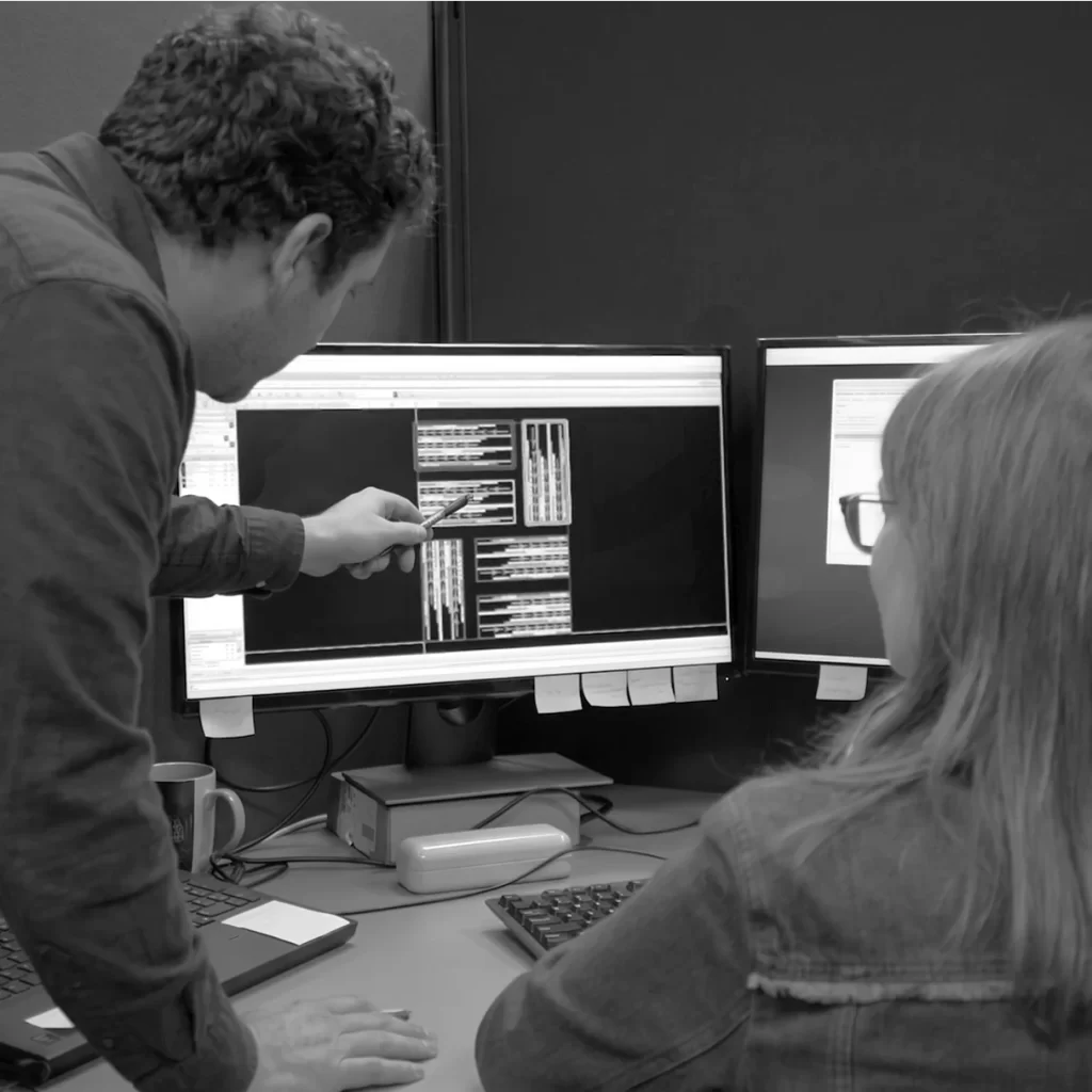
Integration Expertise Across Technologies
Explore Our Technologies
-

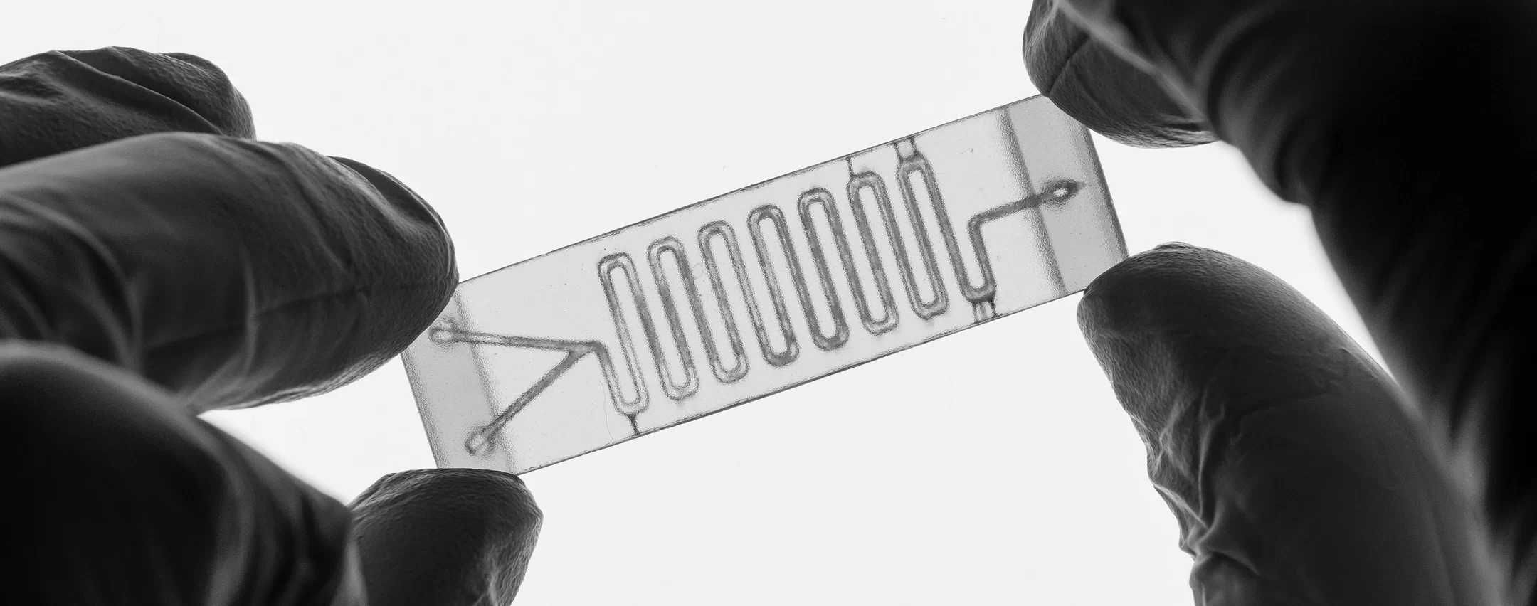
Enabling a Broad Range of MEMS-Based Devices
Learn MoreAdvanced fabrication capabilities support fluidic nanochannels and other MEMS structures with feature sizes down to 40nm. SkyWater supports the development and manufacturing of diverse MEMS technologies, including:
- Actuators, micro-motors
- Biosensors and microfluidics
- CMUTs
- Gas/chemical sensors
- Infrared detectors: microbolometers, thermopoiles
- Micro-speaker, electrostatic
- Pressure sensors
- Resonators
-
Photonics Expertise Built for Commercialization
Learn MoreSkyWater supports the development of complex photonic devices featuring high-aspect-ratio structures and sub-micron geometries, including diffraction gratings with pitches down to 0.28μm. Our domestic development and production environment helps customers move advanced photonic technologies from research to market with confidence:
- Detectors
- Fiber couplers
- Grating couplers
- Modulators
- Waveguides
-

CMOS for Advanced System Integration
Learn MoreSkyWater combines proven automotive-grade CMOS technologies with advanced integration capabilities to enable next-generation smart sensors, heterogeneous systems, and monolithic device architectures. Our 90nm and 130nm platforms provide a flexible foundation for integrating diverse technologies:
- Silicon interposers
- Wafer-to-wafer oxide and hybrid bonding
- Fine-pitch fan-out wafer-level packaging (FOWLP) roadmap
- Smart sensor integration
- CNFET-based SoC development

Advanced Process Technologies
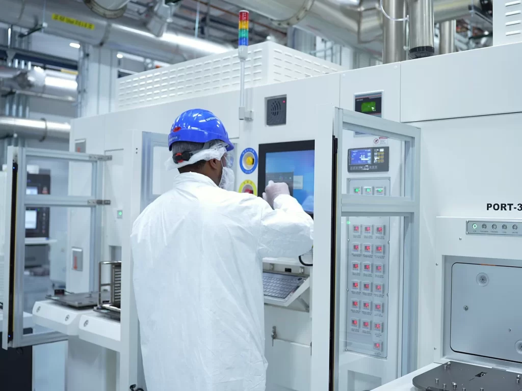
A broad portfolio of process modules enables the development of highly differentiated MEMS, photonic, sensing, and custom device architectures.
Capabilities include:
- High-aspect-ratio etching (DRIE)
- Conformal thin-film deposition
- Thick metals and electroplating
- Thick photoresist processing
- Wafer bonding technologies
- Nanostructure fabrication
- Nanochannel formation
- Advanced lithography and patterning

Engineer What’s Next in MEMS + Photonics
Whether you’re developing a novel sensor, integrated photonic device, biomedical platform, or breakthrough microdevice architecture, SkyWater provides the integration expertise, development infrastructure, and manufacturing foundation to help bring it to market.