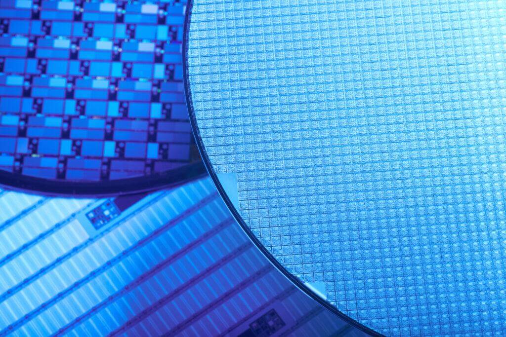
Rapidly verify concepts in a production fab.
Get started in four easy steps:
- Submit your contact information.
- Discuss your project with a SkyWater technologist.
- Download PDK to begin work.
- Co-create your technology with SkyWater to guide you through completion.
We are currently accepting design submissions for the following Multi Project Wafer programs. Connect with us for schedule details and shuttle features.
The S90LN flow includes low noise performance transistors and features that enable infrared imaging and other sensor array applications. The program is ideal for specialized aerospace and defense applications, LIDAR and LADAR, automotive sensing, microbolometers and medical x-ray, augmented reality, industrial machine vision and security, among others.
RH90 is a 90nm fully depleted silicon-on-insulator complementary metal-oxide-semiconductor process specifically developed to produce electronics which can withstand radiation environments. The MPW shuttle standard process flow features a Cu BEOL for M1-M5 and aluminum for M6-M7.
Scroll for More
MPW Schedule
| Year | ID | Technology | GDS Submission | GDS Cutoff |
|---|---|---|---|---|
| 2025 | MPW RH90 #15 | RH90 | 11/29/25 | 12/13/25 |
| 2026 | MPW S130 #25 | S130 | 1/1/2026 | 1/15/2026 |
| 2026 | MPW S90LN #15 | S90 LN Rev1 | 2/1/2026 | 2/15/2026 |
| 2026 | MPW S130 #26 | S130 | 4/1/2026 | 4/15/2026 |
| 2026 | MPW S90LN #16 | S90 LN Rev1 | 5/1/2026 | 5/15/2026 |
| 2026 | MPW RH90 #16 | RH90 | 6/3/2026 | 6/17/2026 |
| 2026 | MPW S90LN #17 | S90 LN Rev1 | 8/2/2026 | 8/16/2026 |
| 2026 | MPW S90LN #18 | S90 LN Rev1 | 11/1/2026 | 11/15/2026 |
| 2026 | MPW RH90 #18 | RH90 | 11/29/2026 | 12/13/2026 |
Sophisticated Design Tools
- PDK, DDK for 90nm and 130nm design rules
- Proven IP over billions of devices
- I/Os and standard cells for logic synthesis
- Silicon proven IP – billions of devices made
- IP licensing available for 130nm SONOS NVM
- IP ecosystem hosted in XENA cloud