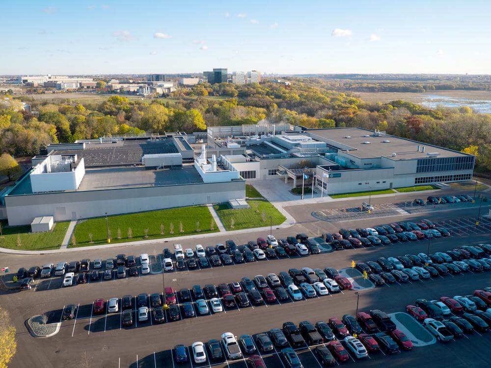
Minnesota Fabrication Facility & Capabilities
Recently expanded in 2020 to enable additional capacity and Cu back end of line, our headquarters boasts a rich heritage of technology development and quality volume manufacturing.
- 200 mm equipment
- 91,000 sq ft cleanroom (class 10)
- Capacity: 10,000 30 ML CMOS wafers/month or 50,000 MOSFET wafers/month
- 90 nm + feature geometries
SkyWater Minnesota Site Certifications

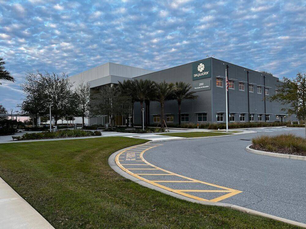
Florida Fabrication Facility & Capabilities
Through a partnership with Osceola County, Florida, SkyWater is now the sole operator of the state-of-the-art Center for Neovation where we are onshoring the next generation of advanced packaging.
- 200 mm equipment
- 36,000 sq ft cleanroom (class 1,000 & class 10,000)
- Facility will enable custom heterogeneous integration solutions
SkyWater Florida Certifications
SkyWater Process Integration Tools & Capabilities
Metals: AIN, TiN
Oxides: SiO2, Al2O3, HfO2, TiO2, ZrO2
Josephson Junction dep and etch
Stud vias
Ti and Co Silicide
Carbon nanotube dep/pattern/etch
Deep trench and through silicon via
Metal liftoff
Cu dual damascene
W plug dual damascene
Nb damascene
Photo stitching in both X and Y directions, sub-20nm stitching errors
Single die whole wafer capability
Low temp (~200C) back end of line processing
Nitrided gate oxide
ASML I-line stepper
ASML I-line scanner
ASML DUV stepper
ASML DUV scanner
ASML 193nm single stage scanner – 90nm CD
ASML 193nm twin stage scanner – sub 65nm CD
Overlay down to single digit nm
Max field size 26mm x 32mm
DNS 80B track
Sokudo RF3 track
TEL ProZ Lithius track
Photo Metrology
AMAT Verity (multiple versions) CD
AMAT VeraSEM
KLA 5200/5300/Archer overlay
Reticle storage/handler/defect inspection
Advanced Process Control (APC) feed forward and backwards
Lam/Novellus/AMAT
PECVD TEOS, C2 and Producer
– low temp options
PECVD silane oxide/nitride/oxynitride, C1
– low temp, range of R.I. options
PECVD nitride C1
– high R.I., low temp options
Lam/Novellus High Density Plasma (HDP) doped and phos doped with sputter etch
– high aspect (5:1) fill capability
Lam/Novellus PECVD Tungsten
– plug fill
– PNL option for high aspect ratio (up to 10:1)
AMAT PVD Metal
Sputter etch, degas
Aluminum both pure and Cu doped
TiW
ESC TiN
Imp TiN
Collimated Ti
WN
Cobalt
Niobium
SiO2
Electroplating
AMAT Raider single wafer Cu plating
Metal Etch
Lam 9600, Al, TiW, TiN, Pt
Lam 2300 Versys, Al, TiW, TiN, Nb, Pt
Poly/Silicon Etch
AMAT DPSII, HBR, Cl2, NF3, CF4, CHF3, O2
– gate, trench, W/WN
– feed forward and back Advanced Process Control (APC)
Lam 9400 TCP, poly/nitride, HBr, CF4, SF6, O2
Lam 4400, HBr, Cl2, C2F6, CF4, SF6, O2
Resist removal/cleans
Gasonic PEP, remote microwave plasma, N2, O2, 120C – 270C
Iridia RF microwave, N2, O2, H2, CF4, NH3, H2/N2, 40C-270C
Mattson Aspen2, RF plasma, O2, CF4, H2>N2, up to 250C
Akrion Gamma Batch Wet Bench
– Sulfuric, SC1, phosphoric, BOE, spin or IPA dry
Batch Rotational
– EKS265, EKC270 solvents, CO2 injected DI
Single Wafer
– SEZ223, Davinci, HF, DSP+HF, titration controlled
Furnaces/Diffusion/Pre-Clean
Scribe: Lumonics Superclean
Furnaces are all made by Aviza
wet oxidation to 1150C
dry oxidation to 1150C
Ar anneal to 1150C
N2 anneal to 1150C
LPCVD nitride, with NH3 and also DH3
LPCVD polysilicon (undoped), both amorphous and crystalline
LPCVD silane oxide
LPCVD oxide/nitride/oxide
LPCVD BTBAS low temp nitride
Atmospheric selective oxidation
H2 and forming gas alloy
Polyimide cure
Pre-cleaning
DNS wet bench industry standard HF/SC1/SC2
dilute HF-last with IPA dry
FSI Mercury industry standard HF/SC1/SC2 rotational
RTA
Ag Heatpulse 8808 NH3, Ar, N2, O2, up to 1200C
Ion Implant
Axcelis 8250 Mid current B11, BF2, As, ESC chuck, E shower, 1e11 to 1e14, 0-60 deg tilt
Axcelis GSD High current/energy B11, BF2, P, As, 10-3000kev, 1e11 to 5e15, tilt/twist
Axcelis GSD Hi dose B11, BF2, P, As 2-180kev, 5e12 to 5e16, tilt/twist
AMAT Mirra CMP
– oxide
– nitride
– niobium
– aluminum
– tungsten
– high selectivity tungsten
– copper
Track ammonia clean
IPA clean
On board metrology with feed forward and backward
Parametric Test
HP 4062UX
– DC, capacitance, pulse generator, frequency counter
– automatic data upload, SPC, analysis, disposition
Engineering manual Probe Station
Sort
Advantest T5365P
Verigy V3308, V4108
Credence Duo
Credence LT
Fuse GSI M325
Verigy 93000
Camtek Falcon (outgoing QA)
REL Lab
Qualitau
Summit 200 Prober/Tester
PMC200 Cryo Probe
Fab services to streamline the concept-to-production journey.
FEI Dual Beam FIB/SEM
Hitachi S-4800
SELA EM2 Precision Cleave
Oxford PlasmaLab RIE deprocessing
Allied TechPrep polisher
MPW/shuttle processing
Mask GDS to reticle
OPC modeling
Layout support
eTest measurement development
High resistivity, red phos low resistivity and Silison on Insulator processing
Cryogenic probing down to 8-Kelvin