As the advanced packaging community gathers for the 76th IEEE Electronic Components and Technology Conference this week, SkyWater Technology is showcasing its expanding advanced packaging capabilities in the exhibit hall at Booth 1201. With demand for AI infrastructure, high-performance computing, and secure domestic semiconductor manufacturing continuing to accelerate, advanced packaging has become a critical technology for enabling next-generation system performance and heterogeneous integration.
In our recent blog post, SkyWater’s Advanced Packaging CTO Frank Wang shares his perspective on the advanced packaging platforms SkyWater is developing in Florida and how these investments are helping strengthen U.S. supply-chain resilience and secure manufacturing capabilities for commercial and defense applications.
SkyWater Expands Advanced Packaging Capabilities to Support AI and Next-Generation Computing
By Frank Wang, Advanced Packaging CTO, SkyWater Technology
The rapid growth of artificial intelligence (AI), high-performance computing (HPC), and data-intensive workloads is driving unprecedented demand for semiconductor performance. As traditional transistor scaling slows with the deceleration of Moore’s Law, advanced packaging has been playing an increasingly important role to improve bandwidth, latency, power efficiency, thermal management, and system integration.
To address these evolving requirements across commercial markets, the Defense Industrial Base (DIB), and U.S. government agencies, SkyWater Technology is expanding its advanced packaging capabilities at its Florida facility. The company is developing a broad portfolio of technologies that includes silicon interposers for 2.5D integration, hybrid bonding and TSV-last with RDLs for high-density 3D architectures, and Fan-Out Wafer-Level Packaging (FOWLP) for scalable high-performance heterogeneous integration. These capabilities are being developed within a secure DMEA Trusted facility and supported by the growing Florida microelectronics ecosystem, helping strengthen domestic semiconductor manufacturing capacity and supply-chain resilience in the United States.
SkyWater’s strategy is centered on enabling high-density heterogeneous integration, where multiple chiplets across different process technologies can be combined into a single package. Rather than relying on increasingly expensive monolithic devices, advanced packaging allows logic, memory, power management, networking, sensors, RF components, and photonics chips built on processes optimized around each component’s function to be integrated in modular architectures that improve scalability, yield, flexibility, and time-to-market.
SkyWater’s Florida site is working to combine these core platform technologies with specialty process services such as direct wafer bonding, wafer thinning, temporary bond/debond, cavity etch, microbump formation, under-bump metallization (UBM), flip-chip assembly, along with the flexibility to co-develop custom processing to enable unique packaging needs. Together, these capabilities provide customers with a flexible development and manufacturing environment spanning both prototype and production needs.
Silicon Interposers and TSV-Last Integration
As advanced processors continue to increase in complexity, the semiconductor industry is shifting away from large monolithic dies and toward chiplet-based architectures. Silicon interposers have become a foundational technology for enabling this transition because they allow chiplets fabricated on different process nodes to communicate at extremely high bandwidth and very low latency.
This capability is especially important in AI accelerators and HPC systems, where processors must interface closely with High-Bandwidth Memory (HBM). Positioning compute and memory devices side-by-side on a silicon interposer with ultra-fine interconnect paths significantly improves data bandwidth and power efficiency. Silicon interposers also redistribute fine-pitch I/O connections into bump geometries compatible with package substrates while supporting thermomechanical reliability through matched coefficient-of-thermal-expansion (CTE) between the interposer and attached Si dies.
Another important advantage of interposer-based 2.5D architectures is thermal accessibility. Because the active dies remain exposed at the package surface, thermal interface materials (TIMs), heat sinks, and cold plates can be attached readily, enabling improved cooling for high-power AI and compute devices operating at increasingly high thermal design power (TDP).
These advantages are accelerating adoption of silicon interposers across:
- AI accelerators and hyperscale data centers
- High-performance networking systems
- Telecommunications infrastructure
- Advanced Driver Assistance Systems (ADAS)
- Autonomous vehicle compute platforms
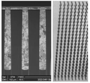 SkyWater has demonstrated a low-leakage TSV-first approach for silicon interposer technology, with a TSV aspect ratio of 10:1 and multiple Redistributed Layers (RDLs) on both sides at min. line / space (L/S) less than 1um, as well as formation of Aluminum pads and Under-Bump Metallization (UBM). The SEM image (left) shows a TSV cross-section before reveal and X-ray image (right) of a TSV array shows high quality control with void-free TSV plating at scale.
As packaging architectures evolve toward 3D integration, however, Through-Silicon Vias (TSVs) are often required directly within active device wafers rather than only within an interposer. Due to process limitations in many device technologies, TSV-first integration is not always feasible, making TSV-last processing necessary. In our TSV-last flow, TSVs are formed from the backside of the completed wafer after front-side device fabrication has been finalized. SkyWater has successfully demonstrated TSV-last integration with reliable etch stop on aluminum pads and void-free TSV fill forming electrical connections into CMOS devices. TSV-last at high aspect ratio and depth > 100um are currently under development, with multiple RDLs, pad structures and UBM built on top of the TSV structure. Combined with wafer thinning and die / wafer stacking processes, TSV-first and TSV-last technologies can support a broad range of advanced 3D integration schemes, including:
- Front-to-front (F2F)
- Front-to-back (F2B)
- Back-to-back (B2B)
- Back-to-front (B2F)
These integration approaches enable increasingly complex heterogeneous systems while maintaining high interconnect density and optimized signal routing.
Hybrid Bonding for High-Density 3D Integration
As interconnect density requirements continue to increase, conventional microbump assembly technologies are beginning to approach their physical limitations. State-of-the-art solder-capped copper pillar approaches typically operate in the 36–45 µm pitch range, constraining bandwidth density, latency, thermal performance, and power efficiency in the next-generation systems.
Hybrid bonding has emerged as a transformative alternative by enabling direct copper-to-copper and dielectric dielectric bonding along the same interface down to sub-micron pitch. This technology supports extremely high interconnect density—exceeding one million IOs per square millimeter—while simultaneously improving bandwidth, latency and power efficiency.
Hybrid bonding obviates the need for solder joints. In particular, the direct Cu-Cu bond structure avoids intermetallic compound formation typically associated with solder joints. Instead of underfill materials, direct dielectric bonding fully seals the interface for improved mechanical stability and environmental protection. These characteristics improve stack-height control, current ampacity, thermal performance and long-term reliability.
In summary, key advantages of hybrid bonding include:
- Extremely high interconnect density
- Ultra-low latency, low power consumption and reduced signal loss
- Improved thermal conductivity
- Minimal assembly force and tight Z-height control
- High throughput enabled by room-temperature initial bond and batch annealing
- High current ampacity and high reliability as compared to solder joints
These benefits are driving rapid adoption of hybrid bonding across advanced memory and imaging applications, including backside-illuminated CMOS image sensors, 3D NAND, SRAM-on-logic architectures, compute-on-I/O systems, and emerging HBM4/5 modules.
SkyWater has partnered with Adeia to offer wafer-to-wafer (W2W) hybrid bonding capabilities, using wafers from different sources. The process flow includes redistribution layer formation and Direct Bond Interconnect (DBI) via and pad fabrication, using a damascene process with precise CMP and dishing optimization, followed by cleaning, plasma activation, hydroxylation, alignment, room-temperature initial bonding, and batch annealing.
Achieving a high bond quality requires exceptionally tight control over:
- Surface flatness
- Dielectric rounding profile
- Copper recess (dishing)
- Particle & contamination control across the bonding surface
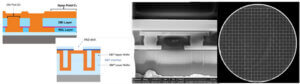
SkyWater has demonstrated void-free hybrid bonding at sub 10um pitch across full wafer area in test vehicles with bond strength measurements exceeding 1.5 J/m² required for downstream processing, as shown in the left side of the figure below where the top and bottom wafers each contain a half daisy-chain and the daisy-chain becomes complete after hybrid bonding. The right side of the figure below shows a cross-section of the hybrid bonded interface with 3um pad size at 8um pitch and the CSAM inspection confirming void-free uniform bond quality across the full wafer area.
Beyond W2W integration, SkyWater plans to expand into Die-to-Wafer (D2W) and Die-to-Die (D2D) hybrid bonding using an automated 300 mm tool scheduled for installation in 2026. These approaches enable the use of Known Good Die (KGDs), improving yield while providing greater flexibility for heterogeneous integration of chips from different sources where materials and processes are tuned for best performance.
In addition to conventional face-to-face (F2F) configuration, these hybrid bonding capabilities can support multi-layer stacking architectures using Face-to-Back (F2B) and Back-to-Back (B2B) integration, in conjunction with TSV-enabled dies.
Fan-Out Wafer-Level Packaging (FOWLP)
Although silicon interposers have enabled major advances in high-performance computing, their scalability is constrained by reticle size limitations, stitching complexity, throughput, and cost—particularly for very large integration areas. These limitations become increasingly critical in AI systems that require large-scale integration of compute, memory and networking devices across expansive package footprints.
FOWLP provides a scalable alternative for heterogeneous integration across large areas without the reticle & stitching constraints associated with silicon interposers. SkyWater’s FOWLP leverages Deca Technologies’ platform including Laser Direct Imaging (LDI) for lithography, which enables large-format patterning without reticles while offering faster prototyping cycles and lower development costs. Unlike conventional stepper lithography, LDI allows arbitrarily large layouts with significant design flexibility and supports 1.5 µm line/space dimensions suitable for many die-to-die interconnect applications. Embedded silicon bridges in dual-sided FOWLP can further extend interconnect density below 0.5 µm line/space, supporting large-scale AI compute and networking systems.
This architecture also enables advanced power delivery through stacked vias in RDLs and vertical via thru the mold, with embedded power modules and integrated voltage regulator (IVR) placed close to compute devices. These approaches help reduce IR drop, lower power delivery network (PDN) impedance, improve energy efficiency, and suppress electrical noise in increasingly complex HPC and AI systems.
For RF and mmWave applications, FOWLP offers several electrical advantages compared with silicon interposers. Relying on low-loss organic mold compounds and polymer dielectrics rather than silicon-based TSV structures, FOWLP features reduced insertion loss, parasitic coupling / crosstalk, and substrate losses at high frequencies. Additionally the platform supports Antenna-in-Package (AiP) integration, making it well suited for compact 5G, radar, automotive, aerospace and defense systems.
In applications with lower I/O density and compact form-factor requirements, FOWLP packages can often be mounted directly to the PCB without an intermediate organic substrate. This shortens electrical interconnect paths, minimizes parasitic effects, and reduces size, weight, power, and cost (SWaP-C).
In summary, key advantages of FOWLP include:
- Scalable large-area integration without reticle limit or stitching complexity
- Lower RF signal loss and crosstalk compared with silicon interposers
- Support for Antenna-in-Package (AiP) features
- Reduced SWaP-C for edge, aerospace, and defense systems
- Flexible heterogeneous integration across large package areas
- Improved power supply using embedded devices and vertical delivery
FOWLP Development and Roadmap
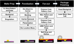 Funded by DoW’s RESHAPE program, SkyWater Florida has secured an effort to onshore 300mm FOWLP packaging technologies. As shown in this image, FOWLP (chip-first approach) process flow starts with building Cu stud on the incoming pads, followed by mold reconstitution, RDLs and UBM, ball attach and singulation. Ref. DOI:10.1109/ECTC51909.2023.00033
SkyWater’s chip-first FOWLP technology incorporates Adaptive Patterning™ from Deca Technologies to compensate for die shift and rotation during high-density assembly. This single-sided FOWLP platform will roll out first and the baseline design kit will support up to 5 redistribution layers with 2 µm minimum line/space dimensions and 20 µm I/O pitch meeting the needs for Chip-Scale Package (CSP) and Multi-Chip Module (MCM). Dual-sided FOWLP development (with up to 4 layers of RDL on each side) is progressing in parallel and will enable vertical power delivery and signal routing from backside to frontside, and 3D stacking of multiple dies or FOWLP packages using Copper Post Via (CPV) structures through the mold compound and stacked via through RDLs.
SkyWater’s FOWLP development roadmap highlights include:
- Q3 2026: Early-access PDK for single-sided FOWLP
- Q4 2026: Early-access PDK for dual-sided FOWLP
- Q2 2028: Full qualification of advanced FOWLP platforms
Compared with TSV-based 3D stacking approaches, dual-sided FOWLP can provide greater design flexibility by eliminating the constraints associated with TSV location, size and clearance zones as well as the matched chip sizes in case of W2W bonding. This becomes particularly valuable in applications where TSV integration is impractical due to stress concerns or design-space limitations within CMOS devices.
Specialty Manufacturing Services
To complement its advanced packaging platforms, SkyWater is expanding its specialty process offerings to support both die-level and package-level integration.
Current development efforts include the following capabilities expected to be available in 2027:
- Solder-capped copper pillars for fine-pitch microbump assembly
- UBM and C4 solder ball attachment over 200mm and 300mm wafer area
Business Model and Design Enablement
SkyWater supports customers through two complementary engagement models. Wafer Services focuses on production manufacturing using mature technologies and qualified PDKs, while Advanced Technology Services (ATS) emphasizes collaborative process development and technology customization through structured, phase-gated engineering programs from prototype through production with rigorous risk management and qualification methodologies.
To support increasingly complex heterogeneous systems, SkyWater is also establishing a unified co-design ecosystem spanning circuit and package design, packaging, board-level integration, IP integration, and multi-physics simulation. This environment is intended to enable System-Technology Co-Optimization (STCO) while improving system performance and power efficiency, signal integrity (SI), power integrity (PI) early in the product development cycle through Design for Manufacturability (DFM), Design for Reliability (DFR) and Design for Testability (DFT). Meanwhile SkyWater is working through the domestic supply chain in partnerships with substrate manufacturers and OSATs to support customers’ needs at the system level. Combined with in-line and off-line inspection, metrology, testing, and failure-analysis infrastructure, these capabilities position SkyWater well to support turnkey solution for the interested customers.
Looking Ahead
SkyWater Florida is building an open-access advanced packaging ecosystem designed to support customers across commercial, aerospace & defense, and governmental markets. By combining flexible platform technologies, secure manufacturing, process customization, co-design enablement, and domestic supply-chain partnerships, SkyWater aims to accelerate the deployment of advanced heterogeneous integration solutions driving innovation for AI and next-generation computing.
Visit SkyWater at Booth 1201 during ECTC 2026 to learn more about the company’s advanced packaging roadmap and manufacturing capabilities.