VORAGO Technologies to Move All its Manufacturing Stateside in Strategic Partnership with SkyWater’s Trusted Foundry

SkyWater to implement VORAGO’s patented HARDSIL® technology that enhances performance of radiation-hardened and radiation-tolerant devices used in commercial, aerospace and defense applications

BLOOMINGTON, Minn. and AUSTIN, Texas – January 24, 2023 – SkyWater Technology (NASDAQ: SKYT), the trusted technology realization partner, today announced a strategic partnership with VORAGO Technologies, effectively moving VORAGO’s fabrication efforts stateside to SkyWater’s DMEA-accredited Category 1A Trusted Foundry. The partnership is based on SkyWater implementing VORAGO’s patented HARDSIL® technology, which is a cost-effective semiconductor processing method that enables devices to operate at higher temperature and radiation levels.

With this implementation, HARDSIL will be available to SkyWater customers as a design-enabled processing method for new or existing designs without any impact on die size, specification, and without redesign. HARDSIL will enhance SkyWater’s bulk 90 nm CMOS process for commercial use in space, aviation, industrial, and medical applications that require higher levels of radiation tolerance.

In contrast to standard commercial design and manufacturing processes, high-reliability radiation-hardened (rad-hard) electronic components must be designed and manufactured so that exposure to ionizing radiation and/or extreme temperatures does not result in malfunctions or catastrophic failure. VORAGO offers innovative technology which enables meeting rad-hard performance without requiring design changes – eliminating or reducing the need for costly and time-consuming adjustments or modifications.

Recently, the U.S. has made the strengthening of domestic semiconductor manufacturing capabilities a major priority. As the semiconductor industry experiences silicon shortages, SkyWater’s fab and VORAGO’s technology are positioned to domestically source these important components for use in commercial as well as aerospace and defense applications.

“Partnering with a U.S.-based pure-play foundry is an incredible milestone for us,” says Bernd Lienhard, CEO of VORAGO Technologies. “We’re excited to move all of our manufacturing to SkyWater, the foundry of choice for our next-generation of rad-hard processors. We’re proud to work with SkyWater to bring our patented HARDSIL technology to the aerospace and defense industry at large.”

“We are pleased VORAGO has chosen SkyWater as its preferred foundry,” said Thomas Sonderman, president and CEO of SkyWater. “Implementing their HARDSIL technology enhances our bulk 90 nm CMOS process by enabling applications in commercial and other markets that require high levels of radiation tolerance. VORAGO’s choice to move all their manufacturing to the U.S. is commendable as the nation continues its reshoring efforts for national and economic security.”

About HARDSIL® Technology
HARDSIL is a patented, node-, foundry- and product-agnostic solution utilizing a few additional implant modules based on standard fab equipment, allowing for the fabrication of rad-hard electronic components. Specialized design libraries or major process modifications are not necessary, allowing foundries to transparently re-use existing IP, design libraries and flows. HARDSIL easily incorporates exceptional rad-hard capability into standard semiconductor IC creation. HARDSIL is a cost-effective modification to commercial process flows that can be implemented quickly with minimal incremental mask and implant steps. VORAGO has developed multiple products using HARDSIL and it has been used under license by other leading semiconductor suppliers.

About VORAGO Technologies
VORAGO Technologies is a privately held, high technology company based in Austin, Texas with over 15 years of experience in providing radiation-hardened and extreme-temperature solutions for the Hi-rel marketplace. VORAGO’s patented HARDSIL® technology uses cost-effective high-volume manufacturing to harden any commercially designed semiconductor component for extreme environment operation, and has created a number of solutions throughout Aerospace, Defense and Industrial applications, with a proven flight heritage. VORAGO has been named as one of Inc.’s 5000 Fastest Growing Companies in the US. VORAGO Technologies opens up a new world of possibilities for your designs, no matter how hostile the environment. www.voragotech.com

About SkyWater Technology
SkyWater (NASDAQ: SKYT) is a U.S.-owned semiconductor manufacturer and a DMEA-accredited Trusted supplier. SkyWater’s Technology as a ServiceSM model streamlines the path to production for customers with development services, volume production and heterogeneous integration solutions in its world-class U.S. facilities. This pioneering model enables innovators to co-create the next wave of technology with diverse categories including mixed-signal CMOS, ROICs, rad-hard ICs, power management, MEMS, superconducting ICs, photonics, carbon nanotubes and interposers. SkyWater serves growing markets including aerospace & defense, automotive, biomedical, cloud & computing, consumer, industrial and IoT. For more information, visit: www.skywatertechnology.com.

SkyWater Technology Forward-Looking Statements
This press release contains “forward-looking” statements within the meaning of the Private Securities Litigation Reform Act of 1995, including statements that are based on the Company’s current expectations or forecasts of future events, rather than past events and outcomes, and such statements are not guarantees of future performance. Forward-looking statements are subject to risks, uncertainties and assumptions, which may cause the Company’s actual results, performance or achievements to be materially different from those expressed or implied by such forward-looking statements. Key factors that could cause the Company’s actual results to be different than expected or anticipated include, but are not limited to, factors discussed in the “Risk Factors” section of its annual report on Form 10-K and quarterly reports on Form 10-Q, and in other documents that the Company files with the SEC, which are available at http://www.sec.gov. The Company assumes no obligation to update any forward-looking statements, which speak only as of the date of this press release.

VORAGO Technologies Contact: Hadley Hempel | hhempel@voragotech.com
SkyWater Company Contact: Tara Luther | 952.851.5023 | tara.luther@skywatertechnology.com
SkyWater Media Contact: Lauri Julian | 949.280.5602 | lauri.julian@skywatertechnology.com
Re-shoring Heterogeneous Integration Technologies

By Alan Huffman, heterogenous integration business unit director

Supply chain constraints have jumped into headlines in recent years as challenges associated with surging demand and pandemic-related disruptions have turned sourcing strategies upside down. The microelectronics industry has been in the spotlight on numerous occasions owing to major shortages in the automotive industry. This has put a mainstream spotlight on issues known to many industry insiders for years – many key manufacturing technologies for the microelectronics value chain have been entirely offshored. While for years it was an abstract vulnerability — for most, when consumers cannot get products they want or need, it very quickly becomes a household issue with real implications for us all.

As a result, there is growing momentum to “re-shore” many of the microelectronic manufacturing capabilities that migrated out of the United States over the past 20 years. Not only does this help to strengthen the nation’s supply chain capabilities, but it also supports many national security initiatives to ensure that the United States maintains an advantage in microelectronics technologies. This initiative is considered so important that Congress is working on a significant funding program called the United States Innovation and Competition Act. While many of the conversations around re-shoring microelectronics manufacturing technologies center around the most advanced and smallest geometries produced by the likes of TSMC, Intel and Samsung, it also acknowledges that perhaps one of the most striking gaps in our domestic infrastructure is for packaging technologies, which is a segment of the supply chain basically abandoned by major U.S. suppliers.

In January 2021, SkyWater took over operation of the Center for Neovation, a state-of-the-art 200 mm semiconductor manufacturing facility in NeoCity, Osceola County to address emerging commercial and government agency needs for U.S.-sourced electronics.

As a country and industry, how did we get here?

Prior to 2000, much of the innovation for advanced packaging came from IDM companies (e.g. IBM, Intel, Motorola) and OSATs (e.g. Amkor, ASE). As the market shifted from high-end computing toward the very high-volume mobile market, cost was the major driver for packaging. This resulted in packaging manufacturing migrating to lower-cost countries, mainly in Asia, while high value innovation resources in the U.S. were focused on advanced node technology development and design for processors.

This led the industry to extend established packaging technologies to accommodate the low-cost objectives of the market, which was achieved very well. Over the last decade, advanced packaging technology advancements began to be driven by leading foundries (TSMC, Samsung, Intel) and OSATs, as packaging technologies have been increasingly relied on to help maintain the pace of performance increase in electronic systems.

In 2016, TSMC introduced a wildly successful fan-out wafer-level packaging, called InFO, that was used by Apple for packaging processors in a low-profile package and is still used in their package-on-package designs for mobile devices today. This example shows the impact of 2.5 heterogenous integration architectures on mainstream applications. Now as we see a slowdown in performance gains by conventional Moore’s Law transistor scaling, the industry is in unanimous agreement that the future of advanced computing will proceed hand-in-hand with heterogenous integration technologies in order to meet the market’s incessant demand for more performance. However, with advanced packaging supply chain infrastructure being virtually non-existent in the U.S., where does that leave us?

The current paradigm shift the industry is fording — taking the industry from the smartphone era to the parallel and edge computing era that will be enabled by advanced hybrid computing architectures. It marks a shift, where packaging technologies previously viewed as non-performance enhancing low-value services, now are critical enablers for system performance, and can create substantial differentiation for products. A significant opportunity exists for the industry and domestic supply chains to re-establish onshore capabilities in technologies that will enable advanced systems in the coming decades.

What SkyWater is doing about it

SkyWater is in the process of implementing three new technology capabilities to establish the company as a domestic leader in heterogeneous integration: silicon interposers, hybrid bonding and fanout wafer level packaging — also known as FOWLP. These platform technologies form the basis of SkyWater’s commitment to establishing leading edge capabilities to support the “More than Moore” generation of microelectronics that the industry will rely on for the future.

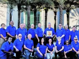
The SkyWater team celebrates the completion of the first high density interconnect test vehicle which represents the phase one goal of the federally funded Industrial Base Analysis and Sustainment program with Bridg.

Silicon interposers can be thought of as a very advanced circuit board. They utilize silicon microcircuit processes to form multiple layers of routing metal and incorporate through silicon vias, or TSVs, to create an integration platform that allows for extremely short interconnect lengths between the devices assembled to them and provides connections through the silicon to allow for electrical signals to be transmitted from the bottom to the top of the interposer.

Through a technology agreement between Bridg and IMEC, SkyWater is establishing silicon interposer manufacturing in our Florida facility. Interposers are key components used in the integration of multiple devices in very close proximity to one another. High performance computing modules that need intimate integration between logic and memory are an example of an application where interposers play an important role. Interposers are also used for the integration of “chiplets,” which are silicon devices designed to perform a specific function and work together with other chiplets in microsystems.

Bridg is a not-for-profit public-private partnership organization supporting research and development focused on advanced system integration solutions. SkyWater’s silicon interposer technology is based on work done at IMEC, a leading microelectronics research organization in Belgium. In cooperation with Bridg, SkyWater is establishing the manufacturing capabilities to support high-volume silicon interposer fabrication.

Through an agreement with Deca Technologies, developer of the industry-leading FOWLP technology, SkyWater will be establishing the first high-volume FOWLP capability in the U.S. Deca’s first generation FOWLP technology is used extensively in leading mobile applications and their proprietary Adaptive Patterning, with mask-less laser direct imaging lithography, enables high production yields and high-density design rules. SkyWater and Deca are working together to bring Deca’s Gen 2 FOWLP technology to the Florida facility for high-performance computing and networking, artificial intelligence, and edge computing applications. The Gen 2 technology will enable up to 4 routing metal layers with line and space dimensions down to 2 microns and support device die I/O pad pitch down to 20 microns.

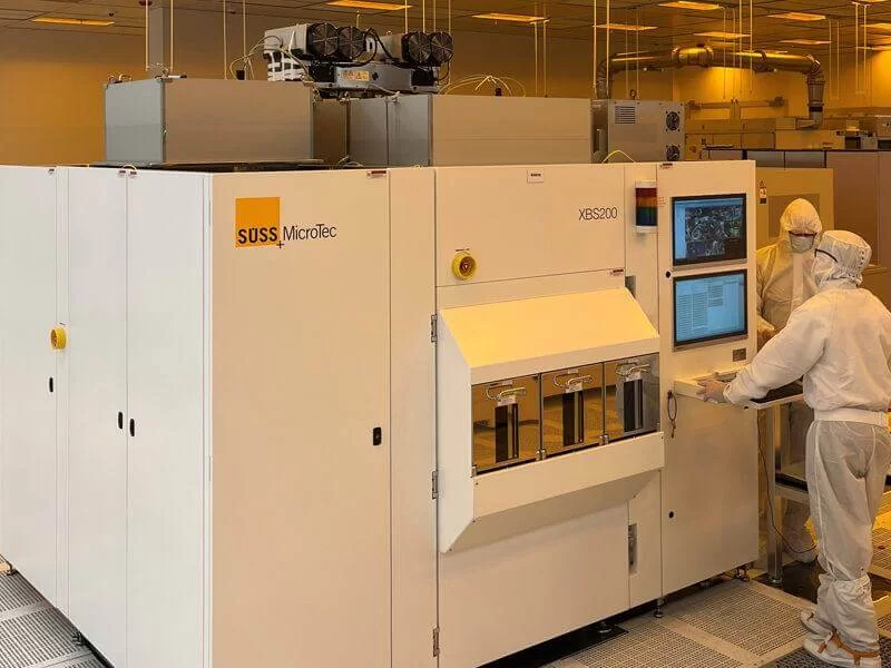
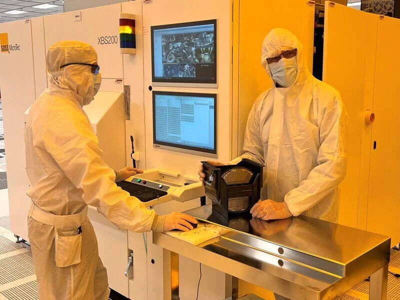
An automated SUSS MicroTec wafer bonder has been installed and direct bonding process development is underway at SkyWater Florida.
The SkyWater Florida facility has achieved ISO 9001: 2015 Quality Management System certification to support domestic heterogenous integration solutions. As part of the certification process, SkyWater Florida engaged in a rigorous audit of its business processes.

Hybrid bonding is the final heterogeneous integration platform technology that SkyWater is implementing, via a licensing agreement with Adeia (part of Xperi). While silicon interposer and FOWLP are HI technologies that primarily integrate devices in the horizontal direction with vertical off-module signal transmission paths, hybrid bonding enables true 3D integration of devices and allows them to be stacked directly upon each other. This approach allows for very short interconnection lengths between devices, resulting in lower power consumption, higher bandwidth and extremely compact device size.

Through the course of our work enabling disruptive innovators across diverse technology categories, we’ve observed firsthand the need for new back end of line integration architectures in order to maximize device performance. The addition of these advanced technologies to enable 2.5D and 3D architectures provides our customers with a one-stop shop for development and manufacturing services that span front and back end of line technologies and with the IP security of a domestic foundry partner.

With growing market demand for heterogeneous integration and advanced packaging technologies — and broad local, state and national government support for re-shoring them in the U.S. — a great opportunity is presented to the U.S. supply chain for regaining leadership for the next generation of packaging technology. We’re ready for the challenge and looking for partners who are hungry to innovate with us.

Learn more about Heterogeneous Integration