SKY’s the Limit with the SKY130 Open-Source PDK

The open-source ecosystem sparks innovation, lowers barriers to chip design and paves a new path for global workforce development

by SkyWater CTO Steve Kosier

Three years ago, SkyWater, Efabless and Google teamed up to release the industry’s first open-source foundry Process Design Kit, or PDK, known as SKY130 — based on SkyWater’s volume 130 nm CMOS technology. The partnership gave designers worldwide free access to chip design technology to create new, manufacturable designs. While the focus of this effort was largely on revolutionizing technology realization for all — some exciting social developments also emerged.

Interested in an update, we sat down with SkyWater’s Chief Technology Officer Steve Kosier to talk about the SKY130 PDK — curious to learn how it’s helping the innovation ecosystem globally while introducing chip design skills to an organically developing talent pipeline — with free educational tools for anyone interested in developing a skillset as a chip designer.

The huge cost of chip design stifles innovation and cripples education

Semiconductor design costs grow exponentially with each new node. To use commercial tools and design a production-ready 130 nm chip, you can expect to spend about $5,000,000. Migrate to 65 nm, and you’ll need $20,000,000. If we move to the leading-edge technology, 5 nm, the bill can be as much as half a billion dollars. For 2 nm is even more expensive at $725,000,000. Obviously, such figures put chip design out of reach for an individual user.

There are other barriers to chip design too. You need Electronic Design Automation, or EDA tools, non-disclosure agreements, intellectual property agreements, access to fabrication and testing. For many aspiring chip designers, organizations, and creators of new products — these hurdles can be insurmountable.

In educational institutions, access to chip design tools that target manufacturable process flows can be limited and unaffordable — leaving students with theoretical knowledge but lacking practical experience. Furthermore, the inability to share information between institutions, reference prior designs by other researchers, or afford wafer fabrication makes educating and attracting students to semiconductor careers difficult.

What if the cost was closer to $0?

Enter the value proposition for open-source PDKs. Open source tools are free to all, which eliminates the cost to get started — unleashing creativity and making chip design available to more people. The Google-sponsored Open Multi Project Wafer, or Open MPW, Shuttle Program attracted designers from academia, commercial organizations and beyond, enabling market-relevant designs to be fabricated by people who traditionally would not have had the opportunity to design a chip.

In the first MPW run in 2020 there were 42 submissions and about 60% of the designs were submitted by non-chip design experts — demonstrating a significant untapped interest generated by putting design capability in the hands of non-traditional users. In subsequent MPW runs, the submission rate grew to 162 in 2021 and 418 in 2022.
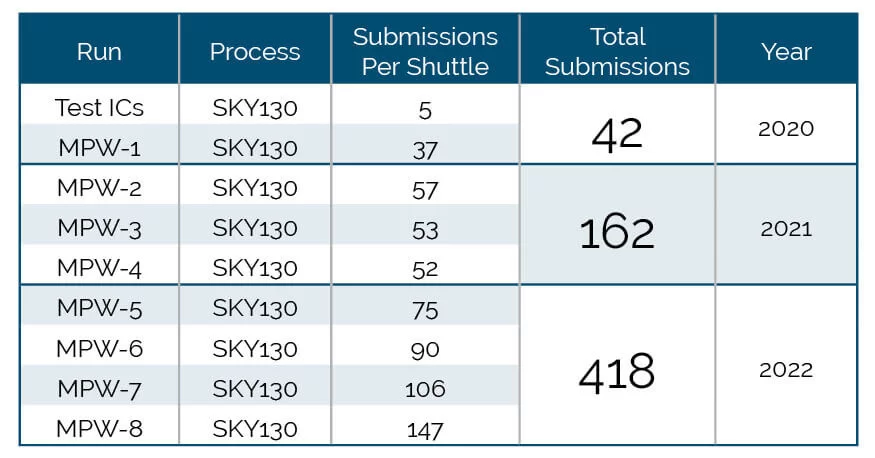
How did it all come together? SkyWater licensed the technology to Google who then released the PDK and funded eight MPW shuttles. This was in collaboration with our partner, Efabless, who delivered the engineering platform, design aggregation, and developed key intellectual property.

No-cost tools and low-cost fabrication is democratizing high-end silicon design
Our partner in this effort, Efabless, provides ChipIgite which consists of Caravel, a pre-designed carrier-chip along with an automated open-source design flow called OpenLane, making creating a chip easy and affordable. This rapid path to prototyping and low-volume production is ideal for educational institutions, startups, and individuals who want to design market-relevant products.

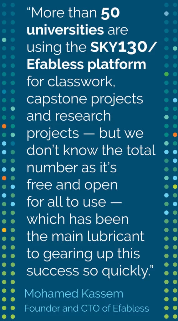
Co-founder and CTO of Efabless Mohamed Kassem explains, “The number of institutions of learning on SKY130 is rapidly increasing. More than 50 universities are using the SKY130/eFabless platform for classwork, capstone projects and research projects — but we don’t know the total number as it’s free and open for all to use — which has been the main lubricant to gearing up this success so quickly.”

In some cases, students who take such classes use slots on a ChipIgnite, which will be fabricated by SkyWater. ChipIgnite is scheduled in April, June, September and November so that students get silicon back the following session to test and demonstrate projects with working implementations.

All users appreciate:

  • No legal agreements — All students, researchers, and professors access foundry technology, chip reference designs, EDA tools and design flows that are completely open-source. There are no NDAs or other legal requirements. All content can be downloaded from git repos. URL https://skywater-pdk.readthedocs.io/en/main/
  • No export control restrictions — This makes it easy to provide access for all people.
  • Freedom to collaborate — Share design files across teams and organizations, including GDS final layout files.
  • Rapid design — Complete a design in a full chip within a single course or cycle of learning by leveraging reference designs and automated flows. By using the Caravel SoC on SKY130, it’s possible to complete a focused design goal quickly.
  • Tiny Tapeout – This program allows a designer to go from idea to chip design in minutes. A student can now do a design for $50. An eight-year-old created a chip using this innovation.
  • New research-focused tools — A new NIST and Google Nano Accelerator and Open Cryo PDK built on the SKY130 platform delivers the scale of open IP and multi project wafers to the research community.
  • MPW shuttle program – The Google-funded MPW shuttles helped get this program started. While those initial eight shuttle runs have concluded, programs like Tiny Tapeout and ChipIgnite are available for designers to design and manufacture affordably.


130 nm CMOS is a proven workhorse for mixed-signal applications and ideal learning node

Opening development on this widely used and commercially relevant node is ideal because it has a large pool of existing IP given its maturity — something that’s valuable for seasoned and novice chip designers alike. The more advanced the node, the more design rules — and the longer it takes to validate and manufacture a chip.

One university professor who started teaching with SKY130 moved to a 16 nm node platform for a semester. She has returned to SKY130 saying that it was too hard for first-time chip designers to complete a chip using the 16 nm alternative. SKY130’s simplicity and compatibility with early education is essential to giving students a practical experience where they can learn and successfully create a chip.

A talented community is building the future in the “Innovation Tail”

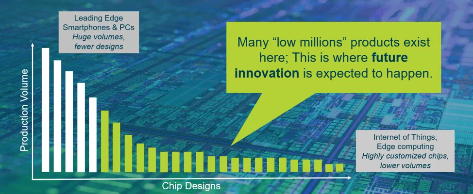
The greatest chip production volumes serve leading edge applications such as smartphones, PCs, memory, etc. While they have huge volumes — they also have very few designs. On the other end, there is a very long tail where many millions of products exist. This is where future innovation is happening. It makes sense to make technology accessible to all so that we can improve what’s there and grow the knowledge base of the world.
 

Since SkyWater released its open source SKY130 PDK there are now more than 6,400 members in the Slack interactive discussion workspace and membership continues to grow! There are also 100+ channels including #analog-design, #courses and #riscv. The best part is that anyone can join here.

On Google-sponsored shuttle MPW-8, the fastest ever design creation rate emerged. A remarkable 147 unique market-ready manufacturable designs were submitted in a lottery for free fabrication. Although only 40 designs could be chosen for fabrication, the work and designs are still available for all to reference, use and improve.

There were many interesting designs submitted including sleep apnea devices, a flu detector, smart garden and image detection at the edge. These innovative designs speak to the whole purpose of the ecosystem: people can come up with their designs and share them with the world.

We need more people interested in semiconductor careers
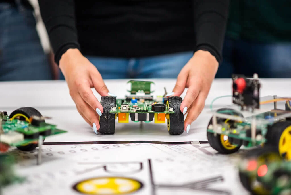
One of the challenges facing the semiconductor industry is a shortage of talent. As technology continues to advance, the demand for skilled professionals in semiconductor design and fabrication is growing. To address this issue, we need to capture the attention of younger students —those entering high school — to increase awareness earlier. In addition, we need to emphasize the value of semiconductor careers and make education and training more accessible.

Open-source initiatives can play a pivotal role in workforce development by providing learning resources and hands-on experience opportunities for aspiring semiconductor professionals. We couldn’t do this before because of the large barriers to entry. Now with open-source, there are no questions. We can create textbooks, share resources, and create programs of learning that benefit everyone.

Start designing today at Efabless.com or Tiny Tapeout

The open-source revolution in semiconductor design is transforming an industry once shrouded in exclusivity into one that welcomes innovation from all corners of the globe. By lowering the cost of design tools, enabling affordable fabrication, and fostering a global community of chip designers, the open-source ecosystem is democratizing high-end silicon design.

In fact, SkyWater recently announced the availability of a new Cadence open-source PDK and reference design which will be available in the Cadence® Very Large-Scale Integration Fundamentals Education Kit. The kit teaches students how theories and concepts can be applied in the design of simple logic circuits and in the physical implementation of a simplified microprocessor. This is exciting news, and we anticipate more announcements like this soon.

It is inspiring seeing everyone using and making improvements to the SKY130 PDK. It takes everyone working together to improve the community and advance the state of open-source tools. If you have ever wanted to design a chip, now you can. It’s never been easier to get started.

I would encourage you to investigate the SKY130 PDK. Who knows — your design could solve a key problem, move rapidly to volume production, and improve the world!

SkyWater to Provide Foundry Service for new NIST and Google Partnership to Create Supply of Chips for Researchers and Tech Startups

Appoints Brian Lenihan vice president of government relations to build upon SkyWater’s strategic initiatives in support of the CHIPS Act

BLOOMINGTON, Minn. – September 15, 2022 – SkyWater Technology (NASDAQ: SKYT), the trusted technology realization partner, today announced it will manufacture chips that researchers can use to develop new nanotechnology and semiconductor devices through a cooperative research and development agreement between the U.S. Department of Commerce’s National Institute of Standards and Technology (NIST) and Google. Through the partnership, Google will pay the initial cost of setting up production and will subsidize the first production run. NIST, with university research partners, will design the circuitry for the chips. The circuit designs will be open source, allowing academic and small business researchers to use the chips without restriction or licensing fees.

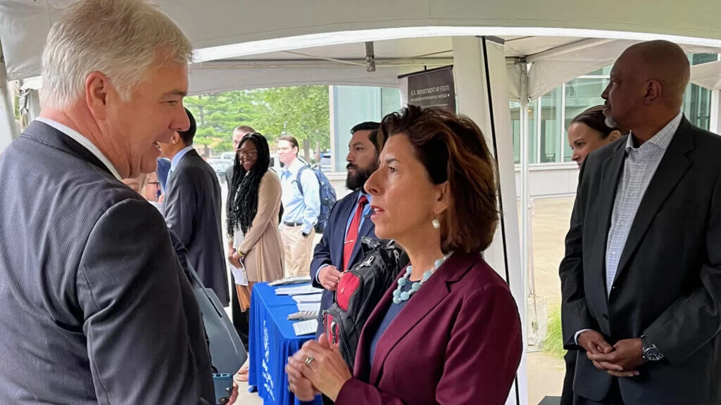
SkyWater President and CEO Tom Sonderman talks with U.S. Secretary of Commerce Gina Raimondo at an event at Purdue University on Tuesday, September 13, 2022.

“It was exciting to hear Secretary Raimondo announce the partnership between NIST, SkyWater and Google during her visit to Purdue this week, along with Secretary Blinken, Senator Young and Indiana Governor Holcomb to discuss the role of universities in CHIPS Act funding related to microelectronics research, manufacturing and workforce development,” said SkyWater President and CEO Thomas Sonderman.

SkyWater has a history of public-private partnerships and will continue that success with the appointment of Brian J. Lenihan to the role of vice president of government relations, based in Washington D.C. Lenihan brings extensive public policy experience and will be focused on deepening the company’s relationships within all levels of government, highlighting SkyWater’s value as the only U.S.-owned pure-play foundry. He will play a key role in leading government relations initiatives in support of the CHIPS Act to further U.S. innovation, workforce development and secure manufacturing.

Vice President of Government Relations Brian Lenihan

“Brian joins SkyWater following his efforts in the Department of Commerce and NIST to drive public policy forward for the microelectronics industry, and now he will leverage his expertise to enhance SkyWater’s offerings to our customers and the country,” said Sonderman. “We are pleased to have a leader of Brian’s caliber and capability join SkyWater’s ranks to continue the efforts we have achieved so far. He will be key to our success, especially at this time, when effective engagement with stakeholders has never been more important to enhance America’s standing in the most advanced technologies.”

Prior to SkyWater, Lenihan served in a variety of public and private roles within the government affairs realm, as a presidentially appointed senior executive in positions at the U.S. Department of Commerce. Previously serving as the executive director of SelectUSA, the U.S. government’s business investment agency, he also held roles as senior advisor in the offices of the Secretary, Deputy Secretary and other agency leaders, including chief of staff at NIST. In addition to his roles in the Executive Branch, Lenihan led regulatory and federal affairs for trade associations and served as a legislative aide to three respected and senior members of the U.S. House of Representatives. He received his B.A. in political science from the University of Central Florida.

“SkyWater is at the leading-edge of microelectronics, co-developing differentiated products with its customers using its unique Technology as a Service (TaaS) business model and is particularly well-positioned in delivering critical technologies for our Nation’s security,” said Lenihan. “I am thrilled to work with SkyWater colleagues to build upon their achievements and to work with our partners and stakeholders to advance the goals of the company and our country to build truly foundational opportunities for economic growth, national security, and advanced technological innovations.”

About SkyWater Technology
SkyWater (NASDAQ: SKYT) is a U.S.-owned semiconductor manufacturer and a DMEA-accredited Trusted supplier. SkyWater’s Technology as a ServiceSM model streamlines the path to production for customers with development services, volume production and heterogeneous integration solutions in its world-class U.S. facilities. This pioneering model enables innovators to co-create the next wave of technology with diverse categories including mixed-signal CMOS, ROICs, rad-hard ICs, power management, MEMS, superconducting ICs, photonics, carbon nanotubes and interposers. SkyWater serves growing markets including aerospace & defense, automotive, biomedical, cloud & computing, consumer, industrial and IoT. For more information, visit: www.skywatertechnology.com.

SkyWater Technology Forward-Looking Statements
This press release contains “forward-looking” statements within the meaning of the Private Securities Litigation Reform Act of 1995, including statements that are based on the Company’s current expectations or forecasts of future events, rather than past events and outcomes, and such statements are not guarantees of future performance. Forward-looking statements are subject to risks, uncertainties and assumptions, which may cause the Company’s actual results, performance or achievements to be materially different from those expressed or implied by such forward-looking statements. Key factors that could cause the Company’s actual results to be different than expected or anticipated include, but are not limited to, factors discussed in the “Risk Factors” section of its annual report on Form 10-K and quarterly reports on Form 10-Q, and in other documents that the Company files with the SEC, which are available at http://www.sec.gov. The Company assumes no obligation to update any forward-looking statements, which speak only as of the date of this press release.

SkyWater Company Contact: Tara Luther | 952.851.5023 | tara.luther@skywatertechnology.com
SkyWater Media Contact: Lauri Julian | 949.280.5602 | lauri.julian@skywatertechnology.com

SkyWater Receives Funding from DOD, Partners with Google to Facilitate Open Source Design for its new 90 nm Technology Offering

Open source program enables a pipeline for IP creation, accelerates innovation and provides a pathway to volume production

BLOOMINGTON, Minn. – July 28, 2022 – SkyWater Technology (NASDAQ: SKYT), the trusted technology realization partner, today announced it is receiving $15 million in funding from the Department of Defense (DOD) to facilitate open source design for its 90 nm process offering, part of the previously announced $27 million investment. To enable this initiative, SkyWater has partnered with Google, through Google Public Sector and company-wide engineering teams, to build on its commitment to open source silicon. SkyWater previously announced a partnership with Google to enable open source design of custom application-specific integrated circuits (ASICs) on its 130 nm mixed-signal CMOS process through the open source SKY130 PDK.

SkyWater’s new commercial SKY90-FD open source offering is based on MIT Lincoln Laboratory’s 90 nm fully depleted silicon on insulator (FDSOI) CMOS process technology. Through this latest government funded program at SkyWater, innovation that is enabled by open source design is focused on commercial use of this technology.

According to Dr. Matthew Kay, DOD program manager for this project, “Investments in commercial endeavors such as the partnership between SkyWater and Google is another example of how the Department of Defense can leverage technology advancements within the open source community to effectively and efficiently improve our defensive posture for the future.”

The DOD is using many OSS (Open Source Software) programs which play a growing role in mission-critical systems and defense applications that must perform repeatedly and reliably. Open source accelerates innovation through cumulative efforts and fosters trust due to its transparency, which enables identification of design flaws and malicious code, something that is not always possible with proprietary software. This use of open source has greatly improved technology and furthered the state of the art in the defense of the United States.

Google has a long-standing history of supporting open source silicon as both a founding member of the RISC-V Foundation and the Linux Foundation’s CHIPS Alliance project, along with an active role in the Open Compute Foundation. The open source model taps into a talent pool of software engineers to design chips in code and run design simulations that test, optimize, and validate specific chip designs. As a result, chip designers are able to iterate and innovate faster, and they have more frequent tape-outs than previously realized through more traditional models. Google became involved in open silicon with the goal of driving down cost over time and reducing barriers to entry for hardware startups and small businesses.

“Through this important investment from the DOD and collaboration with Google, we will enable open source design for our commercial SKY90-FD process technology, creating an IP pipeline and pathway to commercial volume manufacturing,” said SkyWater President and CEO Thomas Sonderman. “This will expand our 90 nm foundry offering as a platform for innovation and productization here in the U.S.”

“Our public-private partnership with the DOD and SkyWater enables a new era in accessible, collaborative chip design that will be driven by an open source ecosystem,” said Will Grannis, CEO of Google Public Sector. “Our collaboration will help address the historical limitations of chip design and production for national defense by improving accessibility for researchers and developers to innovate faster and at lower costs. Google provides the compute, engineering know-how and platform that accelerates chip design; SkyWater provides the next-gen chip design system and fabrication in a secure commercial environment; and the DOD investment makes this all scalable and accessible.”

For technical information on the SkyWater-Google open source initiative, please visit: Google Open Source Blog (googleblog.com).

About SkyWater Technology
SkyWater (NASDAQ: SKYT) is a U.S.-owned semiconductor manufacturer and a DMEA-accredited Trusted supplier. SkyWater’s Technology as a ServiceSM model streamlines the path to production for customers with development services, volume production and heterogeneous integration solutions in its world-class U.S. facilities. This pioneering model enables innovators to co-create the next wave of technology with diverse categories including mixed-signal CMOS, ROICs, rad-hard ICs, power management, MEMS, superconducting ICs, photonics, carbon nanotubes and interposers. SkyWater serves growing markets including aerospace & defense, automotive, biomedical, cloud & computing, consumer, industrial and IoT.  For more information, visit: www.skywatertechnology.com.

SkyWater Technology Forward-Looking Statements
This press release contains “forward-looking” statements within the meaning of the Private Securities Litigation Reform Act of 1995, including statements that are based on the Company’s current expectations or forecasts of future events, rather than past events and outcomes, and such statements are not guarantees of future performance. Forward-looking statements are subject to risks, uncertainties and assumptions, which may cause the Company’s actual results, performance or achievements to be materially different from those expressed or implied by such forward-looking statements. Key factors that could cause the Company’s actual results to be different than expected or anticipated include, but are not limited to, factors discussed in the “Risk Factors” section of its annual report on Form 10-K and quarterly reports on Form 10-Q, and in other documents that the Company files with the SEC, which are available at http://www.sec.gov. The Company assumes no obligation to update any forward-looking statements, which speak only as of the date of this press release.

SkyWater Company Contact: Tara Luther | 952.851.5023 | tara.luther@skywatertechnology.com
SkyWater Media Contact: Lauri Julian | 949.280.5602 | lauri.julian@skywatertechnology.com