A Closer Look Inside SP90
A common photonics platform for diverse challenges
Brought to you by the SP90 platform architects: Mihir Bhaskar, Bart Machielse, Skylar Deckoff-Jones, Tin Komjlenovic, Jeremy Sage, and Andy Bonifas
Over the past decade, our team has pioneered new frontiers in quantum photonics, using integrated photonics to address challenges in scaling quantum technology. Our work spans on-chip visible-wavelength lasers, integrated diamond quantum memories, thin-film lithium niobate single-photon frequency converters, cryogenically compatible low-loss fiber couplers, and integrated photonic ion traps.
Take it from us: we understand both the tremendous potential of these technologies and the challenge of making them work in a useful quantum system.
This is where SP90 comes from. We’ve worked on a variety of quantum photonics problems, each with different materials, wavelengths, and requirements. They share one common challenge: building a photonic circuit that’s fundamentally different from the traditional telecom and datacom silicon photonics stack. Quantum hardware has unique requirements for color, coherence, memory, loss, and operating environment.
SP90 is our way of addressing that common challenge. Step one is a backend compatible 200 mm silicon nitride (SiN) platform designed to move light at visible to near-infrared wavelengths with low loss. Next comes the material that brings whatever unique capability your system needs: advanced heterogeneous integration and packaging, added in a modular way. You can build photonic integrated circuits with functionality tailored to your device requirements wavelengths, and operating conditions. And in every engagement: advanced engineering and domain specific knowledge from the quantum experts at SkyWater to bring your device from first prototype to world wide deployment.
Following the recent introduction of SkyWater Quantum Solutions, we’re now sharing a closer look at SP90’s optical technologies and wafer-scale characterization, including representative fabricated wafers and devices. This is an early sneak peek. We’ll share more data and capability details over the coming months. But SP90 wafers have already shipped, and customer engagements are moving forward. You can talk directly with our team today about module readiness, design capabilities and access, and delivery timing.
Photonic integrated circuits designed for your needs
SP-CORE is the routing backbone of SP90. The supported optical wavelength range is 400–2000+ nm. We use different SiN thicknesses for different wavelength bands, with multilayer options for circuit design. Photonic building blocks include bends, splitters, crossings, rings, Mach–Zehnder interferometers, edge couplers, and heaters.
We think SP-CORE is a great product. But it’s not “the point” of our photonics platform. Your hardest photonics challenges need more than routing. That’s why we designed the SiN foundation to use backend compatible deposition and processing to support integration with additional layers needed for specific applications.
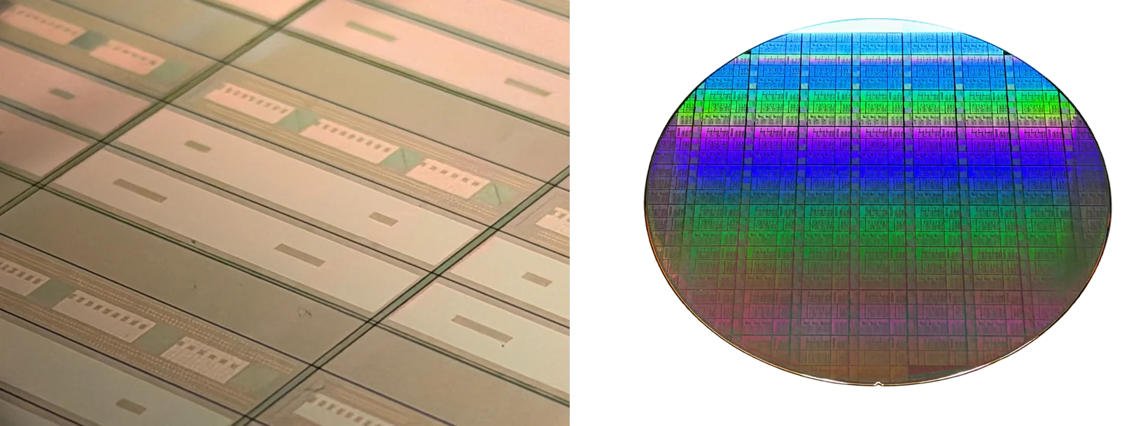
Left: Silicon nitride SP-CORE dies as part of a larger 200 mm wafer.
Right: Photograph of a full 200 mm SP90 wafer, with custom layers for ion trapping added.
Characterizing performance across the wafer
Before we get ahead of ourselves on advanced capabilities, we have to talk about characterization. Wafer-level testing and spatial mapping help us understand device behavior and variation across 200 mm wafers. That’s a requirement for any mature foundry process. We’ve all made our first “hero device.” Now we need to show that we can make it consistently across a wafer, then combine it with more advanced elements.
Our wafer-under-test video on the SP90 product page shows this work in progress. The figure below shows propagation-loss maps at 493, 650, and 1762 nm, with 45 measured die locations per map. It also includes film metrology from a separate 25-wafer physical vapor deposition (PVD) study. These results are preliminary and sample-specific.
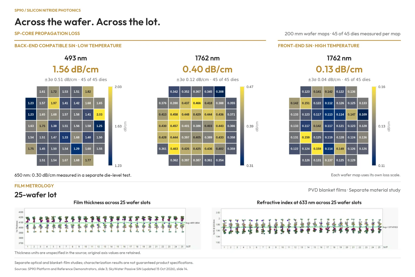
Wafer-scale characterization at two optical wavelengths and for two types of nitride (top), with thickness and refractive-index measurements from a separate 25-wafer PVD film study (bottom). Each optical map uses its own loss scale. Results are preliminary and are not guaranteed product specifications. Loss performance is still being optimized across the 400–2000+ nm range. We will continue to publish updated data as it becomes available.
Full platform characterization and optimization are underway, and we’ll share more as the work progresses. Through SkyWater Quantum Solutions, we also offer photonics characterization services tailored to your wavelengths and requirements.
Advanced optical capabilities
Routing gets light where it needs to go. The next step is to generate, manipulate, store, or detect it. SP90 combines the SiN foundation with technologies for optical I/O, light generation and modulation, diamond memory integration, photon counting, and nonlinear optics. Here’s how we think about each one.
SP-LAS active III-V. Many applications need more than passive components. Lasers and detectors can live off-chip and couple via fiber, but that solution begins to run out of steam if you need a scalable number of channels that can be individually modulated or detected. Trapped-ion, neutral-atom, and photonic quantum computing architectures are racing toward this bottleneck. Quantum networking and sensing have arguably already hit it. SP-LAS is designed to address this issue: it combines III-V gain material with SiN photonics for visible-wavelength light generation and amplification, with individually modulated channels and high extinction. III-V modulators on SiN have been demonstrated at 780 nm and 1 µm. Integrated monitor photodiodes provide optical power readout. For quantum computing, networking, and sensing, this provides a pathway to addressing the laser control bottleneck.
SP-NBN photon counting. For single-photon detection, we want to bring the detector to the light already traveling on the chip. SP-NBN integrates superconducting niobium nitride nanowire single-photon detectors (SNSPDs) with SiN waveguides for photon counting at cryogenic temperatures. This builds on over a decade of superconducting materials fabrication expertise at SkyWater and more than two decades of experience making superconducting nanowire single-photon detectors. Optical coupling and electrical readout are part of the system design. SNSPD wafers without waveguide coupling are also available.
SP-NLO nonlinear optics. The wavelength a quantum device needs may be different from the wavelength you want to send through fiber or the wavelength of your core laser system. In fact – some visible quantum-relevant wavelengths even have no known diode solution. Bulk crystals for frequency conversion based on periodically poled lithium niobate are an effective solution, but do not scale well to many channels. SP-NLO uses thin-film lithium niobate for nonlinear frequency conversion and electro-optic modulation. For quantum networking, the goal is to connect quantum-device wavelengths with the telecom band, alongside the SiN routing and packaging that carry the light. For controlling quantum computers and sensors, SP-NLO is designed to work alongside SP-LAS to provide a scalable light source at wavelengths down to 400 nm.
SP-DIA diamond integration. Diamond hosts solid-state quantum networking and sensing technologies. SP-DIA brings bonded quantum-grade diamond membranes together with SiN routing, with interlayer couplers that move light between the two materials. This connects the diamond structures used for quantum memory and sensing to a photonic circuit that can be manufactured at scale.
SP-PKG optical I/O. Getting light on and off the chip is part of your system’s loss budget. SP-PKG uses tapered-fiber interfaces to couple optical fibers to on-chip SiN waveguides. We can adapt the coupling and packaging to your wavelength and operating conditions. We like our approach better than a typical grating coupler because it can achieve much lower loss. We have reproducibly demonstrated losses below 0.2 dB at visible wavelengths. We also like our approach better than edge couplers: in addition to lowering loss, it can preserve valuable space at the edge of the chip, It supports packaging that maintains low insertion loss as your chip cools from room to cryogenic temperatures, and it mechanically withstands cryogenic cycling. That said, we can offer grating and edge couplers for your architecture if you need them.
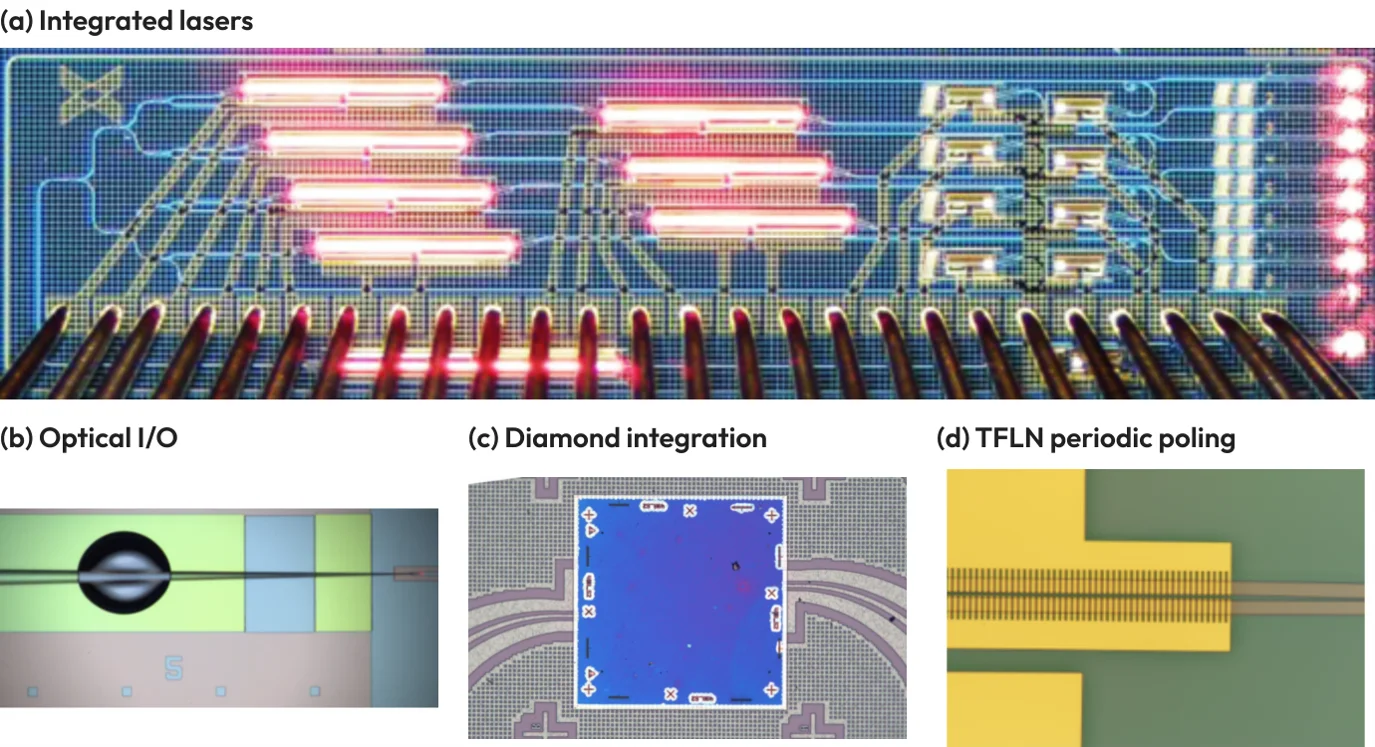
Representative devices and optical interfaces: (a) integrated lasers, (b) fiber-to-waveguide coupling, (c) diamond on silicon, and (d) periodically poled thin-film lithium niobate.
Each combination requires its own integration and validation work. Importantly, the constituent technologies have been brought to SkyWater by the experts who first pioneered them. We know better than any how these technologies work from design to device all the way to a working system. A program around your application
A quantum sensor may need a few integrated lasers, a modulator, and a wavemeter. A quantum network may need to connect a memory to telecom fiber through a frequency converter. A detector program may prioritize coupling efficiency and uniform performance across a wafer. We start with what your system needs to do, then define how to build, characterize, and validate it..
Tell us your wavelengths, loss budget, and operating conditions, together with your development schedule. We can then define the baseline process, integration work, and characterization your program needs.
Most importantly, when you work with SkyWater, your innovation remains yours. We help you manufacture it.
If you would like to discuss your SP90 program, email us at quantum@skywatertechnology.com
Explore SP90: https://www.skywatertechnology.com/sp90-photonics/
Note to Investors Regarding Forward-Looking Statements
This post contains forward-looking statements. All statements contained in this post other than statements of historical fact are forward-looking statements, including statements regarding availability of more data and details in the near future, performance and results of our technologies, timeline for a fully qualified platform. In some cases, you can identify these statements by forward-looking words such as “expected,” “project,” “can,” “will,” “pathway,” “underway” and other similar expressions. These statements are only predictions based on our expectations and projections about future events as of the date of this post and are subject to a number of risks, uncertainties and assumptions that may prove incorrect, any of which could cause actual results to differ materially from those expressed or implied by such statements, including, among others, those described under the heading “Risk Factors” in our annual Report on Form 10-K for the year ended December 31, 2025 and our Quarterly Report on Form 10-Q for the quarter ended June 30, 2026 filed with the Securities and Exchange Commission. New risks emerge from time to time, and it is not possible for our management to predict all risks, nor can management assess the impact of all factors on our business or the extent to which any factor, or combination of factors, may cause actual results to differ materially from those contained in any forward-looking statement we make. Investors are cautioned not to place undue reliance on any such forward-looking statements, which speak only as of the date they are made. Except as otherwise required by law, we undertake no obligation to update any forward-looking statement, whether as a result of new information, future events or otherwise.