SkyWater Technology and Multibeam Corporation Form Partnership to Deploy Multibeam’s Innovative MEBL System

Advanced lithography technology to serve as a key enabler for SkyWater’s domestic foundry roadmap to 45 nm

SANTA CLARA, Calif. and BLOOMINGTON, Minn. – November 18, 2020 – SkyWater Technology, the trusted technology realization partner, and Multibeam Corporation, the maskless lithography technology leader, today disclosed a partnership to deploy Multibeam’s Multicolumn Electron-Beam Lithography (MEBL) system into SkyWater’s newly expanded fabrication facility in support of SkyWater’s roadmap to advance its manufacturing capabilities and accelerate growth. The ground-breaking MEBL system, set to launch in 2021, will be capable of full-wafer, all-maskless patterning at 45 nm and beyond.

“As a Trusted Foundry, we take great pride in meeting stringent security and quality criteria,” said Thomas Sonderman, president and chief executive officer of SkyWater. “We seek innovative solutions that can add high value while reducing manufacturing cost and cycle times; MEBL’s deployment will benefit all of our customers, both government and commercial. Further, this key capability will support SkyWater’s pursuit of a unique foundry offering by combining the flexibility and agility of 200 mm manufacturing with the advanced performance of 45 nm process technology.”

According to David K. Lam, chairman and chief executive officer of Multibeam, SkyWater represents a showcase customer that can take full advantage of MEBL’s high-mix production capabilities. He noted that MEBL greatly simplifies patterning processes, adding, “In product development, MEBL cuts prototyping cost and time because ‘respins’ no longer require a new set of masks. Since all e-beam columns in our MEBL system write independently and in parallel, they empower production of multi-project wafers and chips larger than the typical optical field of view. Our versatile MEBL system design has a throughput capability that extends significantly beyond single e-beam approaches to support volume manufacturing.”

Security Lithography

As a proprietary maskless platform, MEBL can be applied to ensure “security lithography” by embedding unique security information into each IC during routine wafer fabrication. Multibeam’s Secure Chip ID enables chip traceability throughout its lifecycle as well as the confirmation of its unique identity and provenance. Technology development is well under way for the MEBL platform to hardcode unique chip ID into each IC during fabrication – a most secure and cost-efficient way to thwart IC counterfeiting.

About SkyWater Technology

SkyWater is the only U.S.-owned and U.S.-based pure play semiconductor foundry and is a DOD-accredited Trusted supplier, specializing in custom technology development services and volume manufacturing for integrated circuits and micro devices. Through its Technology Foundry model, SkyWater’s world-class operations and unique processing capabilities enable mixed-signal CMOS, power, rad-hard and ROIC solutions. SkyWater’s Advanced Technology Services empower development of superconducting and 3D ICs, along with carbon nanotube, photonic and MEMS devices. The company serves customers in growing markets such as aerospace & defense, automotive, biomedical, cloud & computing, consumer, industrial and IoT. For more information, please visit: www.skywatertechnology.com/.

About Multibeam Corporation

Multibeam is a leader in multicolumn electron-beam lithography (MEBL). With a robust IP portfolio comprising 43 patents, Multibeam is building MEBL production systems and developing applications under DOD contracts. The company targets applications such as high-mix production lithography, complementary e-beam lithography (CEBL), security lithography, and applications in which MEBL holds competitive advantages and offers compelling benefits to semiconductor chipmakers. Multibeam is led by David K. Lam, the founder and first CEO of Lam Research. Widely recognized as a key contributor to the growth of the semiconductor industry, Lam was inducted into the Silicon Valley Engineering Hall of Fame in 2013. For more information, visit:  www.multibeamcorp.com

SkyWater Company Contact: Tara Luther | 952.851.5023 | tara.luther@skywatertechnology.com

SkyWater Media Contact: Lauri Julian | 949.280.5602 | lauri.julian@skywatertechnology.com

Multibeam Contact: Ted Prescop| 408.980.1800 | tprescop@mulitbeam.com
Google Partners with SkyWater and Efabless to Enable Open Source Manufacturing of Custom ASICs

First open source foundry PDK enables full manufacturing chain for open hardware;

Google-sponsored MPW shuttle program now accepting design submissions

BLOOMINGTON, Minn. and SAN JOSE, Calif. – November 12, 2020 – SkyWater Technology, the trusted technology realization partner, and Efabless, a crowdsourcing design platform for custom silicon, today announced design submissions are now being accepted for a series of Google-sponsored open source Multi-Project Wafer (MPW) shuttles that will run at SkyWater. Through a partnership between Google, SkyWater and Efabless, open source designs selected by the program will be fabricated at no cost to the designers. The MPW program is enabled by the first foundry-supported open source process design kit (PDK) for 130 nm mixed-signal CMOS technologies (SKY130 process). The initiative will enable a complete open source manufacturing supply chain for custom application specific integrated circuits (ASICs) and has been discussed in a series of talks produced by the FOSSi (Free and Open Source Silicon) Foundation including presentations by Google and Efabless.

Google has a strong history of supporting open source silicon through being a founding member of both the RISC-V Foundation and the Linux Foundation’s CHIPS Alliance project. Parthasarathy Ranganathan, distinguished engineer, Google said, “Working through its Open Source Programs Office (OSPO), Google is actively engaged in helping seed the open silicon space, specifically by providing funding, strategic, and legal support to key open hardware efforts including lowRISC and CHIPS Alliance.”

In support of the shuttle program, Efabless has released a complete Apache 2.0-licensed open source RTL2GDS design stack, referred to as openLANE, that supports the SKY130 PDK and is available to designers worldwide. With open source designs and a standardized test harness produced by Efabless that is open and freely available, verification results can be easily and cost-effectively replicated by other designers, enabling a new model to evaluate and iterate on ideas. This community-based model also brings a new and effective approach to product verification and security.

This offering has implications for accelerating innovation in the 130 nm mixed-signal SoC node popular for IoT type applications by removing barriers and obstacles relating to experimentation and collaboration for IC design. The model and its innovative outcomes are extensible to advanced nodes over time.

“Launching the portal for design submission is a milestone in connecting a global community of experts who can openly collaborate to create and verify ASICs and supporting IP,” said Mohamed Kassem, Efabless chief technology officer and co-founder. “The open source model multiplies the collaboration in semiconductor chip design. And this is just the start. Over time we expect to see advanced (and high quality) designs coming from the open source community.”

John Kent, SkyWater executive vice president of technology development and design enablement said, “We expect the new open source foundry PDK to serve as an excellent enablement engine for generating re-usable IP which will amplify idea generation and feed product development that is ongoing in the IoT and industrial space.”

About the Google-sponsored MPW Shuttle Program

The open source foundry PDK is accessible at https://github.com/google/skywater-pdk and by the time of this announcement, has been downloaded more than 1700 times in the past two weeks. Efabless has created a digital portal to enable customers to follow a step by step workflow to submit their designs as candidates for the MPW shuttle. The Efabless portal is active now and will accept designs through November 30, 2020. Efabless will perform license and data integrity checks followed by design rule checking prior to assembling the shuttle. Each shuttle run will have 40 design slots (seats) and the first run is scheduled to launch in Q4 2020. In the case submitted designs exceed the number of seats on a shuttle, designers will be deferred to the next shuttle.

More details about the design submission process and requirements can be found at https://efabless.com/open_shuttle_program or https://www.skywatertechnology.com/mpw/open-source-mpw-program/. To learn more about the SKY130 PDK open source foundry offering, please visit https://skywater-pdk.slack.com/ or contact swfoundry@skywatertechnology.com.

About Efabless Corporation

Efabless.com offers a platform and marketplace that uses open source and community models to make the design and commercialization of ICs simple, inexpensive and accessible to everyone.  Efabless accelerates the development of new products and initial proof of concepts through a novel solution based on configurable open source SoC design templates and automated design generation.  Product developers use this solution to rapidly, cost-effectively and reliably create custom silicon. Chip developers use the solution to dramatically reduce cost and time to market for proof of concept of new and exciting ICs.  Our model is extendible to advanced packaging, software, subsystems and full systems.  Efabless is headquartered in San Jose, California. For more information, visit www.efabless.com.

About SkyWater Technology

SkyWater is the only U.S.-owned and U.S.-based pure play semiconductor foundry and is a DOD-accredited Trusted supplier, specializing in custom technology development services and volume manufacturing for integrated circuits and micro devices. Through its Technology Foundry model, SkyWater’s world-class operations and unique processing capabilities enable mixed-signal CMOS, power, rad-hard and ROIC solutions. SkyWater’s Advanced Technology Services empower development of superconducting and 3D ICs, along with carbon nanotube, photonic and MEMS devices. The company serves customers in growing markets such as aerospace & defense, automotive, biomedical, cloud & computing, consumer, industrial and IoT. For more information, please visit: www.skywatertechnology.com/. 

Efabless Company Contact: Jeff DiCorpo | 408.896.2078 | jeffdi@efabless.com

SkyWater Company Contact: Tara Luther | 952.851.5023 | tara.luther@skywatertechnology.com

SkyWater Media Contact: Lauri Julian | 949.280.5602 | lauri.julian@skywatertechnology.com

SkyWater Appoints Two New Members to its Board of Directors

Experts from government agencies and the semiconductor industry bring decades of experience to fast-growing technology foundry

BLOOMINGTON, Minn. – October 27, 2020 – SkyWater Technology, the trusted technology realization partner, today announced the appointment of Rear Admiral (U.S. Navy retired) Wendi B. Carpenter and John T. Kurtzweil, CPA, CMA, MBA to its board of directors. This move expands the board from four members to six.

“I’m thrilled to welcome Wendi and John to the board. They have unique skill sets that will complement those of our existing members while bringing new perspectives and tremendous value to the table,” said Gary Obermiller, SkyWater’s chairman of the board. “Wendi’s high-ranking and extensive experience with government agencies and the DOD will be an incredible asset to the company. In addition, we will benefit greatly from John’s impressive semiconductor industry background and financial management expertise serving leading technology companies.”

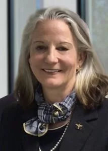
Wendi Carpenter
John Kurtzweil

Wendi Carpenter is currently a principal and founder of Gold Star Strategies, LLC, a consulting company that provides services in strategic planning, organizational transformation, risk assessment, human capital and corporate governance. Previously she served as the tenth president and special envoy and advisor of the State University of New York (SUNY) Maritime College. Prior to SUNY, Ms. Carpenter served as a naval officer in the U.S. Navy, during which she commanded or was the deputy in multiple organizations which oversaw worldwide maritime and air operations, logistics, manpower, installation and facilities management, and training of forces. Her career in the U.S. Navy culminated in the rank of rear admiral.

“I am excited for this opportunity to serve on SkyWater’s board of directors. With its focus on private-public partnerships, SkyWater is leading the charge to bring semiconductor manufacturing back to the U.S. This is evidenced by the DOD’s substantial investment in SkyWater and its recent facility expansion,” said Ms. Carpenter. “I look forward to helping SkyWater continue to innovate and build relationships with both the defense community and commercial organizations.”

John Kurtzweil currently serves as principal of Kurtzweil Consulting, LLC, providing consulting services in the areas of capital formation and accountancy. Previously, he served as vice president of finance and as chief financial officer and treasurer of Cree, Inc., a provider of light emitting diode, lighting and semiconductor products, and chief financial officer of its subsidiary, Wolfspeed. Prior to this, Mr. Kurtzweil served as senior vice president, chief financial officer, and special advisor to the chief executive officer of Extreme Networks, Inc., a provider of open networking innovations. He also served as senior vice president and chief financial officer at Cirrus Logic, Inc., a fabless semiconductor company.

“I’m pleased to join SkyWater’s board of directors and bring decades of experience in the semiconductor industry to this fast-growing, strategic and well-managed company,” said Mr. Kurtzweil. “I’m impressed with how quickly SkyWater has broadened its customer base, enabled by its technology foundry business model that offers technology development and manufacturing in the same secure U.S. facility.”

About SkyWater Technology

SkyWater is the only U.S.-owned and U.S.-based pure play semiconductor foundry and is a DOD-accredited Trusted supplier, specializing in custom technology development services and volume manufacturing for integrated circuits and micro devices. Through its Technology Foundry model, SkyWater’s world-class operations and unique processing capabilities enable mixed-signal CMOS, power, rad-hard and ROIC solutions. SkyWater’s Advanced Technology Services empower development of superconducting and 3D ICs, along with carbon nanotube, photonic and MEMS devices. The company serves customers in growing markets such as aerospace & defense, automotive, biomedical, cloud & computing, consumer, industrial, and IoT. For more information, please visit: www.skywatertechnology.com/.

SkyWater Company Contact: Tara Luther | 952.851.5023 | tara.luther@skywatertechnology.com

SkyWater Media Contact: Lauri Julian | 949.280.5602 | lauri.julian@skywatertechnology.com

SkyWater Commissions Department of Defense-Funded Facility Expansion with Ribbon-Cutting Ceremony and Distinguished Speakers

Officials from the DOD, Department of Commerce, U.S. House of Representatives and local government support SkyWater’s initiative to reshore semiconductor manufacturing

BLOOMINGTON, Minn. – October 23, 2020 – SkyWater Technology, the trusted technology realization partner, today announced that it hosted a ribbon-cutting ceremony last week for its facility expansion that was enabled by a private-public partnership with the DOD. Recent global trade and supply chain dynamics have highlighted the need for domestic sourcing options to improve security for both commercial and national security interests. This SkyWater-DOD collaboration is an example that shows the tremendous potential these types of partnerships can harness to accelerate and enhance domestic manufacturing capabilities.

“Now is the time to build advanced manufacturing technologies to make sure that the infrastructure needed to support the next wave of computing is developed domestically,” said Thomas Sonderman, SkyWater president and chief executive officer.

Over the past few decades, semiconductor manufacturing expertise has been developed and expanded into fabs outside of the U.S. As a result, while today most semiconductor innovation and product development still happen in the U.S., only 12% of the manufacturing is done domestically, according to the Semiconductor Industry Association (SIA). These dynamics are driving federal legislation to facilitate national investment intended for the reshoring of semiconductor manufacturing. As the only solely U.S.-owned pure-play foundry, SkyWater is playing a significant role in leading the return of onshore advanced manufacturing capabilities.

Several government officials presented at SkyWater’s ribbon-cutting ceremony:
• Dr. Jeffrey Nadaner, Department of Defense deputy assistant secretary for industrial policy
• Ian Steff, Department of Commerce assistant secretary for global markets
• Dean Phillips, U.S. representative from Minnesota’s Third Congressional District
• Steve Grove, Minnesota Department of Employment and Economic Development commissioner
• Tim Busse, mayor of Bloomington, Minnesota

SkyWater was also pleased to welcome Dr. Matt Kay from the Department of the Navy, who heads efforts targeting the DOD’s unique needs for microelectronics, and John Neuffer, president and chief executive officer of the SIA, an association which is playing a significant role in the development of legislation to enhance domestic manufacturing.

The DOD’s investment in SkyWater’s facility expansion was made under the Trusted and Assured Microelectronics program, which seeks to collaborate with industry and laboratory partners to provide sustainable, assured technology solutions for national security and defense. While this new portion of SkyWater’s facility was built to enhance microelectronics capabilities for the DOD and the Strategic Rad-Hard market, it will also provide complementary technologies for commercial applications in extreme environments such as space and medical imaging. In addition, the expansion enables SkyWater to add copper interconnect process technology for enhanced mixed-signal device performance and interposer offerings for advanced packaging.

“It’s very good to see industry, government and academia coming together to make events like today possible,” said Ian Steff, Department of Commerce assistant secretary for global markets. “This morning’s tour of the new fabrication facility, which I was very impressed by, is proof that large scale and advanced manufacturing continues to be possible in the United States of America. Our domestic capabilities up and down the supply chain must increase … and will increase. This continues to be enabled by industry-driven approaches with government partnership to improve the investment climate as demonstrated here today.”

“This is an incredibly exciting time for SkyWater and for the semiconductor industry. Now is the time to build advanced manufacturing technologies to make sure that the infrastructure needed to support the next wave of computing is developed domestically,” said Thomas Sonderman, SkyWater president and chief executive officer. “It is because of the vision and leadership of our partners in the Department of Defense that SkyWater and our investors are able to do our part to drive American innovation and grow the domestic high-tech sector.”

A video of SkyWater’s ribbon cutting ceremony is available on the company website’s events page. For more information on SkyWater, please contact: swfoundry@skywatertechnology.com.

About SkyWater Technology

SkyWater is the only U.S.-owned and U.S.-based pure play semiconductor foundry and is a DOD-accredited Trusted supplier, specializing in custom technology development services and volume manufacturing for integrated circuits and micro devices. Through its Technology Foundry model, SkyWater’s world-class operations and unique processing capabilities enable mixed-signal CMOS, power, rad-hard and ROIC solutions. SkyWater’s Advanced Technology Services empower development of superconducting and 3D ICs, along with carbon nanotube, photonic and MEMS devices. The company serves customers in growing markets such as aerospace and defense, automotive, biomedical, cloud & computing, consumer, industrial, and IoT. For more information, please visit: www.skywatertechnology.com/. 

SkyWater Company Contact: Tara Luther | 952.851.5023 | tara.luther@skywatertechnology.com

SkyWater Media Contact: Lauri Julian | 949.280.5602 | lauri.julian@skywatertechnology.com

SkyWater Announces MOU to Provide Domestic Advanced Packaging Capabilities as Reshoring Momentum Builds for Semiconductor Supply Chain

MOU with Osceola County to define terms for SkyWater management of state-of-the-art 200 mm Center for Neovation facility

BLOOMINGTON, Minn. – October 5, 2020 – SkyWater Technology, the trusted technology realization partner, today announced it has entered into an exclusive, non-binding Memorandum of Understanding (MOU) with Osceola County, Florida to explore taking over the lease of the Center for Neovation, a state-of-the-art 200 mm semiconductor manufacturing facility, by forming a new public-private partnership for microelectronics manufacturing and advanced packaging capabilities. Following the MOU, SkyWater, the only U.S.-owned and -operated pure-play Trusted foundry, will define terms with the County to operate the Center for Neovation and utilize the 109,000 square foot facility, with approximately 60,000 square feet of cleanroom laboratory/manufacturing space.

The potential partnership would provide SkyWater tooling capabilities and technologies to enable advanced packaging and heterogeneous integration technology. Today, chip packaging is typically outsourced mainly to Asia. By offering advanced packaging capabilities domestically, SkyWater can enable tighter supply chain management, and deliver increased security and faster time to market for customers. In addition, SkyWater’s strong relationships with government entities will build upon the operation’s success in attracting government programs.

According to Thomas Sonderman, SkyWater president and chief executive officer, “It is our objective to play a significant role in re-domesticating and optimizing technology manufacturing and supply chain management. This potential new public-private partnership with Osceola County is a natural way to extend our capabilities for the defense community and our commercial customers who will benefit from stronger collaboration and integration between domestic foundry and advanced packaging services.”

“SkyWater is an ideal entity to assume management of the Center for Neovation and utilize the specialized capabilities of the facility. As a Trusted foundry, SkyWater is well-equipped to continue existing contracts with the Department of Defense,” said Don Fisher, county manager, Osceola County. “We look forward to the potential of this new relationship to not only develop our region’s technology industry, but to contribute domestic leadership in advanced manufacturing of microelectronics.”

SkyWater and the County of Osceola will have at least 60 days to come to a formal agreement.

About SkyWater Technology

SkyWater is the only U.S.-owned and U.S.-based pure-play semiconductor foundry and is a DOD-accredited Trusted supplier, specializing in custom technology development services and volume manufacturing for integrated circuits and micro devices. Through its Technology Foundry model, SkyWater’s world-class operations and unique processing capabilities enable mixed-signal CMOS, power, rad-hard and ROIC solutions. SkyWater’s Advanced Technology Services empower development of superconducting and 3D ICs, along with carbon nanotube, photonic and MEMS devices. The company serves customers in growing markets such as aerospace & defense, automotive, biomedical, cloud & computing, consumer, industrial and IoT. For more information, please visit: www.skywatertechnology.com/.

SkyWater Company Contact: Tara Luther | 952.851.5023 | tara.luther@skywatertechnology.com

SkyWater Media Contact: Lauri Julian | 949.280.5602 | lauri.julian@skywatertechnology.com

SkyWater Begins Domestic Fab Expansion Tool Installation to Support DOD Investment of up to $170M

Project progresses ahead of schedule and enables first Strategic Rad-Hard MPW shuttles in 2020

BLOOMINGTON, Minn. – September 8, 2020 – SkyWater Technology, the only solely U.S.-owned pure-play foundry, today announced that its facility expansion, supported by the previously announced Department of Defense (DOD) investment of up to $170 million, is progressing ahead of schedule and tool installation has already started. The DOD’s investment was made under the Trusted and Assured Microelectronics (T&AM) program which is developing enhanced sources of microelectronics for the Department’s unique needs. The T&AM program seeks to collaborate with industry and key laboratory partners to provide sustainable, assured technology solutions for national security and defense.

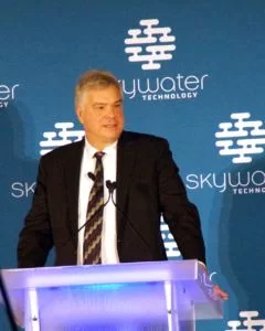
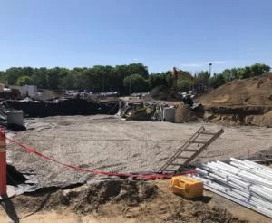
Breaking Ground – October 2019

Less than a year ago, SkyWater announced a multi-phase project to enhance microelectronics capabilities for the DOD and the Strategic Rad-Hard market by expanding its DOD-accredited facility. The expansion will also support complementary technologies for commercial applications in extreme environments such as space and medical imaging. SkyWater is planning to launch its first Early Access Program MPW (Multi-Project Wafer) shuttles before the end of 2020.

Additionally, the expansion will enable SkyWater to add copper (Cu) interconnect process technology for enhanced mixed-signal device performance and interposer offerings for advanced packaging. The new Cu interconnect capability will also be critical in supporting the company’s roadmap for more advanced node geometries beyond 90 nm and aligns well with the growing need for domestic advanced packaging solutions.

Recent global trade and supply chain dynamics have highlighted the disparity between the U.S. dominance in technology innovation and lagging role of semiconductor manufacturing. These dynamics are driving federal legislation to facilitate national investment intended for reshoring critical semiconductor manufacturing elements to improve security for both commercial and national security interests. This expansion of SkyWater’s Bloomington, Minnesota facility is an example of how partnerships between the private and public sector can accelerate the regrowth of onshore advanced manufacturing capabilities.

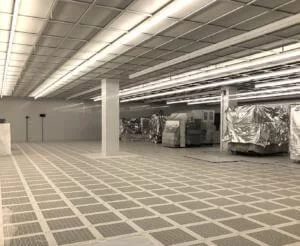
Tool Installation – August 2020

“We are pleased with the progression of work on our facility expansion, especially through the Minnesota winter and this unprecedented pandemic. As an Essential Business, we have safely maintained operations while continuing to serve our government and commercial clients and working to fulfill our commitment to the DOD ahead of schedule,” said Tom Legere, SkyWater Senior Vice President of Operations.

For more information on SkyWater’s new rad-hard process as well as its interposer and high performance mixed-signal offerings, please contact: swfoundry@skywatertechnology.com.

About SkyWater Technology

SkyWater is the only U.S.-owned and U.S.-based pure play semiconductor foundry and is a DOD-accredited Trusted supplier, specializing in custom technology development services and volume manufacturing for integrated circuits and micro devices. Through its Technology Foundry model, SkyWater’s world-class operations and unique processing capabilities enable mixed-signal CMOS, power, rad-hard and ROIC solutions. SkyWater’s Advanced Technology Services empower development of superconducting and 3D ICs, along with carbon nanotube, photonic and MEMS devices. The company serves customers in growing markets such as aerospace & defense, automotive, biomedical, cloud & computing, consumer, industrial, and IoT. For more information, please visit: www.skywatertechnology.com/.

SkyWater Company Contact: Tara Luther | 952.851.5023 | tara.luther@skywatertechnology.com

SkyWater Media Contact: Lauri Julian | 949.280.5602 | lauri.julian@skywatertechnology.com


SkyWater President Thomas Sonderman to Deliver Keynote at 2020 Virtual Advanced Semiconductor Manufacturing Conference (ASMC)

Session to introduce Technology as a Service (TaaS) model to enable disruptive edge and cloud computing technologies that will allow AI throughout the IoT ecosystem

 BLOOMINGTON, Minn., August 20, 2020 – SkyWater Technology, the trusted technology realization partner, today announced the company’s President, Thomas Sonderman will present a keynote address, “Manufacturing Leadership in the Era of Artificial Intelligence,” at the 2020 virtual Advanced Semiconductor Manufacturing Conference (ASMC) at 9:00 am EDT on  August 24th. The presentation will discuss trade and technology dynamics pressuring the manufacturing sector and how a new foundry model can streamline productization for disruptive technologies to enable next-generation edge and cloud-computing infrastructure.

As 5G networks are scaling up, the IoT is rapidly scaling with it and the world is seeing an explosion of IoT devices and unprecedented volumes of data. Artificial Intelligence (AI) technologies with varying sophistication will be critical throughout this expanding ecosystem to realize the value of these data and will rely on continuously progressing compute performance to do so. However, as the industry sees transistor scaling providing diminishing returns, current IC paradigms do not appear suited to deliver the economics or performance the market requires and new dimensions must be pursued including new materials, new architecture, and heterogeneous integration. From a manufacturing standpoint, this is a challenge. Most conventional foundries are not organized with appropriate operational models, tooling, or business processes to innovate efficiently in these new dimensions.

Sonderman’s keynote will address this challenge by presenting a Technology as a Service (TaaS) for microelectronics manufacturing concept that has been demonstrated to facilitate foundry engagement at earlier technology and manufacturing readiness levels and ultimately accelerate time to market. According to Sonderman, “The industry is at an inflection point and the semiconductor manufacturing industry faces a choice between continuing down a known path with reducing returns or chart another path to find new technologies to meet the incessant market demand for more computing performance. The TaaS model is already driving significant innovation in the foundry space for next-wave quantum, cloud, and related computing technologies that will allow the industry to realize the future state of hierarchical AI throughout the IoT ecosystem.”

To attend Sonderman’s presentation, please visit ASMC’s registration page. For more information on SkyWater’s advanced technology and volume manufacturing services, please contact: swfoundry@skywatertechnology.com.

About ASMC

ASMC is the leading international technical conference for discussing solutions that improve the collective manufacturing expertise of the semiconductor industry. Solving the challenges presented by semiconductor manufacturing is a combined effort by device makers, equipment and materials suppliers, and academics. ASMC provides an unparalleled platform for semiconductor professionals to network and learn the latest in the practical application of advanced manufacturing strategies and methodologies.

About SkyWater Technology

SkyWater is the only U.S.-owned and U.S.-based pure play semiconductor foundry and is a DoD-accredited Trusted supplier, specializing in custom technology development services and volume manufacturing for integrated circuits and micro devices. Through its Technology Foundry model, SkyWater’s world-class operations and unique processing capabilities enable mixed-signal CMOS, power, rad-hard and ROIC solutions. SkyWater’s Advanced Technology Services empower development of superconducting and 3D ICs, along with carbon nanotube, photonic and MEMS devices. The company serves customers in growing markets such as aerospace & defense, automotive, biomedical, cloud & computing, consumer, industrial, and IoT. For more information, please visit: www.skywatertechnology.com/.

SkyWater Company Contact: Tara Luther | 952.851.5023 | tara.luther@skywatertechnology.com

SkyWater Media Contact: Lauri Julian | 949.280.5602 | lauri.julian@skywatertechnology.com

SkyWater and MIT Begin Second Phase of DARPA-funded 3DSoC Program; Update to be Presented at Virtual 2020 DARPA ERI Summit

Industry first PDK for CNT-based 3DSoC platform will be available for lead customers in SkyWater’s Early Access Program

BLOOMINGTON, Minn. – August 18, 2020 – SkyWater Technology, the trusted technology realization partner, announced the DARPA Three Dimensional Monolithic System-on-a-Chip (3DSoC) program, in collaboration with Massachusetts Institute of Technology (MIT), has entered its second phase. After completing the program’s initial phase, focused on transferring the Carbon Nanotube Field Effect Transistor (CNFET)-based 3DSoC technology into SkyWater’s 200 mm production facility, phase two will focus on refining manufacturing quality, yield, performance, and density; key elements of commercial viability. The 3DSoC program aims to shift cost/performance benchmarks that have been the standard for decades. This new paradigm is expected to accelerate AI and advanced computing across use cases in autonomous vehicles, medical/healthcare diagnostics, edge computing, wearables, and IoT applications.

The DARPA 3DSoC program, which began in 2018, has realized several technical achievements after running a wide variety of test chips to improve CNT manufacturability and reliability. A 3DSoC program update will be presented by MIT professor, Dr. Max Shulaker at the virtual 2020 DARPA Electronics Resurgence Initiative (ERI) Summit on August 20th. The program team’s work on the 3DSoC program was presented in June at the virtual 2020 Symposia on VLSI Technology and Circuits, highlighting BEOL monolithic 3D integration of CNFETs + RRAM and first hardware demonstrations of the monolithically integrated 3DSoC technology with SRAM and RISC-V compute core. The update also covered the team’s development of an industrial-grade foundry process design kit (PDK) for the 3DSoC technology platform, which marks a significant milestone to enable customer designs in SkyWater’s Early Access Program.

Additionally, the work on foundry integration by MIT and SkyWater was published recently in Nature Electronics demonstrating the methodologies employed to volume manufacture CNTs on 200 mm wafers in the same commercial facilities that fabricate silicon-based transistors. This important step in taking CNTs from the lab to the factory floor paves the way for more energy efficient, 3D microprocessors.

Notably, the technology enables the ability to monolithically integrate stackable tiers of CNT-based logic and RRAM to realize a high-density, high-bandwidth SoC architecture, all with low temperature fabrication techniques. While this is anticipated to accelerate AI and advanced computing, it also opens new dimensions of innovation and potentially enables backend logic integration with non-silicon substrates. This development would bring new possibilities for monolithic heterogeneous integration, which will lead to on-chip logic for new imaging, smart sensors, power management, and many other undiscovered applications.

“We are excited to continue this journey with MIT to fulfill the unique promise of carbon nanotube technology to the semiconductor industry, with disruptive implications for artificial intelligence and leading-edge computing applications across commercial and defense industries,” said Dr. Brad Ferguson, SkyWater Chief Technology Officer.

Added Thomas Sonderman, SkyWater President, “This program is proving the viability and scalability of CNFETs and demonstrates SkyWater’s broader commitment to support the resurgence of advanced manufacturing capabilities in the U.S.”

“It is really exciting to take this giant step forward and hit milestones inside of a foundry environment, making this leap into production. This marks a time for the industry to take notice of CNTs as a much more energy efficient alternative than silicon-based transistors and prepare product roadmaps for this disruptive technology,” said Dr. Max Shulaker, MIT Professor of Electrical Engineering and Computer Science.

An Early Access Program will be offered for chip designers interested in working with SkyWater on this revolutionary and developing foundry offering. Interested parties can submit their information via the program signup page.

About SkyWater Technology

SkyWater is the only U.S.-owned and U.S.-based pure play semiconductor foundry and is a DoD-accredited Trusted supplier, specializing in custom technology development services and volume manufacturing for integrated circuits and micro devices. Through its Technology Foundry model, SkyWater’s world-class operations and unique processing capabilities enable mixed-signal CMOS, power, rad-hard and ROIC solutions. SkyWater’s Advanced Technology Services empower development of superconducting and 3D ICs, along with carbon nanotube, photonic and MEMS devices. The company serves customers in growing markets such as aerospace & defense, automotive, biomedical, cloud & computing, consumer, industrial and IoT. For more information, please visit: www.skywatertechnology.com/.

SkyWater Company Contact: Tara Luther | 952.851.5023 | tara.luther@skywatertechnology.com

SkyWater Media Contact: Lauri Julian | 949.280.5602 | lauri.julian@skywatertechnology.com

John Cooney Named Director of SkyWater’s U.S. Government Relations

Cooney brings extensive policy and government agency experience to support SkyWater’s continued growth initiatives for domestic semiconductor solutions

BLOOMINGTON, Minn. – August 13, 2020 – SkyWater Technology, the trusted technology realization partner, today announced that John Cooney has joined the company from the U.S. Department of Commerce to serve as Director of U.S. Government Relations. He will be focused on deepening the company’s relationships within all levels of government, highlighting SkyWater’s value proposition as the only U.S.-owned pure-play foundry, and addressing opportunities to meet U.S. government needs.

According to Dr. Brad Ferguson, SkyWater Chief Technology Officer and Government Relations Senior Executive, “With over twenty years of experience working at the international, national, and state government levels, John is truly an asset to our aerospace and defense business unit. He will support SkyWater’s unique position as a Trusted supplier and help address the nation’s demand for reshoring the semiconductor industry’s supply chain and restoring American leadership in semiconductor manufacturing.”

Mr. Cooney brings extensive policy and political experience to SkyWater. He most recently served the U.S. Department of Commerce in several positions within the International Trade Administration, including Deputy Assistant Secretary for Global Operations, Deputy Assistant Secretary for Services, and Chief of Staff & Senior Advisor. He has also served in senior roles for members of the U.S. House and the U.S. Senate. Mr. Cooney started his professional career at the Minnesota Legislature focused on small business tax and education legislation. Mr. Cooney graduated from the University of Minnesota with a B.A. in Political Science where he was also a Policy Fellow at the Humphrey School of Public Affairs.

Cooney stated, “I’m excited to join the SkyWater team in my home state of Minnesota, especially at a time when the U.S. government is focusing its efforts to ease heavy dependence on overseas supply chains. I’m looking forward to helping lead the company’s Washington-based and state-based government relations team.”

About SkyWater Technology

SkyWater is the only U.S.-owned and U.S.-based pure play semiconductor foundry and is a DoD-accredited Trusted supplier, specializing in custom design and development services, design IP, and volume manufacturing for integrated circuits and micro devices. Through its Technology Foundry model, SkyWater’s world-class operations and unique processing capabilities enable mixed-signal CMOS, power, rad-hard and ROIC solutions. SkyWater’s Advanced Technology Services empower development of superconducting and 3D ICs, along with carbon nanotube, photonic and MEMS devices. The company serves customers in growing markets such as aerospace & defense, automotive, biomedical, cloud & computing, consumer, industrial, and IoT. For more information, please visit: www.skywatertechnology.com/.

SkyWater Company Contact: Tara Luther | 952.851.5023 | tara.luther@skywatertechnology.com

SkyWater Media Contact: Lauri Julian | 949.280.5602 | lauri.julian@skywatertechnology.com

SkyWater Appoints Srila LaRochelle as Vice President of Strategic Business Development

LaRochelle brings extensive semiconductor industry expertise in product and business development, sales, and strategic marketing

BLOOMINGTON, Minn. – August 3, 2020 – SkyWater Technology, the innovator’s trusted foundry realization partner, today announced that Srila LaRochelle has been appointed as Vice President, Strategic Business Development, bringing extensive semiconductor industry sales expertise to the company, including over a decade of experience at GLOBALFOUNDRIES. In Ms. LaRochelle’s new role, she will focus on supporting SkyWater customers in the western region and will be instrumental in aligning technology roadmaps with strategic customer requirements. She will also focus on new customer engagement in target markets to expand revenue and fab utilization.

Ms. LaRochelle’s experience includes demonstrating effectiveness in product and business development, sales, and strategic marketing within GLOBALFOUNDRIES, UMC, SanDisk, Hitachi, LSI (an Avago Technologies Company) and Harris Corporation. Her education includes earning a BSc in Business Administration and Management from the University of Central Florida and an MBA from Florida Institute of Technology.

“I’m excited to have Srila bring her deep industry experience, market knowledge, and customer engagement expertise to SkyWater allowing us to accelerate our ability to deliver the utmost value to our customers, ensuring their success,” said Mark Litecky, SkyWater’s Chief Revenue Officer.

According to LaRochelle, “I’m very pleased to join SkyWater at this time when the company is growing and evolving so quickly. I look forward to being an integral part of identifying key areas of strategic growth and target markets as well as collaborating within SkyWater to further develop and establish new business relationships.”

About SkyWater Technology

SkyWater is is the only U.S.-owned and U.S.-based pure play semiconductor foundry and is a DOD-accredited Trusted supplier, specializing in custom design and development services, design IP, and volume manufacturing for integrated circuits and micro devices. Through its Technology Foundry model, SkyWater’s world-class operations and unique processing capabilities enable mixed-signal CMOS, power, rad-hard and ROIC solutions. SkyWater’s Innovation Engineering Services empower development of superconducting and 3D ICs, along with carbon nanotube, photonic and MEMS devices. The company serves customers in growing markets such as aerospace & defense, automotive, biomedical, cloud & computing, consumer, industrial, and IoT. For more information, please visit: www.skywatertechnology.com/.

SkyWater Company Contact: Tara Luther | 952.851.5023 | tara.luther@skywatertechnology.com

SkyWater Media Contact: Lauri Julian | 949.280.5602 | lauri.julian@skywatertechnology.com