
Mixed-Signal CMOS
SkyWater’s proven complementary metal-oxide-semiconductor (CMOS) technologies have enabled novel and disruptive products across demanding automotive, industrial, medical and defense markets. As the production foundation, these technologies run in high volume and at world-class quality levels, as demonstrated by numerous quality-driven certifications. But it does not end there: SkyWater’s Advanced Technology Services (ATS) enable the combination of standard CMOS platforms with a wide range of customer-driven additional devices.


Production Proven CMOS Platforms
SkyWater’s 90nm and 130nm CMOS semiconductor manufacturing platforms provide a trusted foundation for established and emerging applications. These mature, high-volume manufacturing platforms have enabled products across automotive, consumer, industrial, biomedical, aerospace, and defense markets, while also serving as the foundation for next-generation innovations in sensing, computing, and advanced electronics.
Applications include:
- Automotive electronics, infotainment, ADAS, and safety systems
- Wearables, smart home technologies, and consumer devices
- Wireless communications and GPS-enabled systems
- Biomedical and DNA sequencing technologies
- Readout integrated circuits (ROICs) for advanced imaging applications
- Emerging memory and compute architectures including CNT, ReRAM, and 3DSoC technologies
Additionally, SkyWater’s advanced 90nm rad-hard by process platform extends these capabilities into the most demanding aerospace, defense, and extreme-environment applications


ThermaView™ ROIC Solutions
Purpose-built CMOS readout integrated circuits that unlock the full potential of advanced infrared detectors and sensor arrays. Designed for applications where performance and reliability matter most, ThermaView delivers low-noise operation, exceptional sensitivity, and trusted domestic manufacturing for aerospace, defense, automotive, and industrial imaging systems.
Multi-Project Wafer Services
Accelerate development with cost-effective access to SkyWater’s Multi-Project Wafer (MPW) programs. Designed for customers evaluating new concepts, validating IP, or preparing for production, MPW shuttles provide an efficient path from design to silicon across our 130nm, 90nm, 90nm ROIC, and RH90 platforms.
SkyWater Design Partner Network
Our design partner network brings together trusted organizations with deep experience across SkyWater technologies, design flows, and manufacturing processes. These proven partners help customers accelerate development, reduce risk, and move efficiently from concept to production through seamless collaboration and specialized expertise.
Platform Data Sheets
SkyWater platforms include PDKs and other essential support with your success in mind. Data sheets are available for the following platforms: S130, S90, S90LN, and RH90 — our advanced radiation-hardened platform for aerospace, defense, and other mission-critical applications.

Robust and Flexible Platforms
for Conventional and Hybrid Solutions
CMOS mixed-signal production process flows are the foundation of our technology offerings. These standard flows and custom variations enable innovators to bring novel ideas to market for silicon and next-wave technologies. Solutions can support conventional SoC and ASIC designs or be combined with your unique idea to create completely differentiated sensor, MEMS, photonics or other structures.
*RH90 is an ITAR restricted technology.
**Operating lifetime depends on operational profile.
| Technology | RH90* | S90/S90LN | S130 |
|---|---|---|---|
| Process | 90nm SOI | 90nm CMOS | 130nm CMOS |
| Wafer Size | 200mm | 200mm | 200mm |
| # Layers Metal and Composition | 1 – 5: Cu 6&7: AI | 7: AI | 5: AI |
| # Layers Local Interconnect | 0 | 2 Dual Damascene | 1 |
| Top Metal | 0.36μm | 0.85 μm | 1.2 μm |
| Mask Steps | 34-36 | 28-38 | 30 – 34 |
| Temperature Range ** (Qualified) | -55° to +125°C Ambient | -55°C to +125°C Junction | -55°C to +125°C Ambient |
| ROIC (Focused Process Option) | No | Yes | No |
| ROIC Die Stitching | No | Yes | No |
| Planarized Viatop | No | Yes | No |
| Cryo Models** (Characterized) | No | 77K to 150K | No |
| Isolation | STI | STI | STI |
| Gate | Co-silicide Poly | W-clad Poly | Poly |
| Core Voltage | 1.2V | 1.2V | 1.8V |
| IO Voltage | 1.8V, 2.5V, 3.3V | 1.8V, 2.5V, 3.3V | 3.3V, 5.0V |
| High Voltage | No | No | 20+V, Drain-Extended CMOS (16V) |
| Multiple Vt Options | Yes | Yes | Yes |
| MiM Capacitor | Yes | 120Ω/□ (N+diff) | Yes |
| Precision Resistor | 195Ω/□ (P-poly) | No | 2000Ω/□ 300Ω/□ (Both P-polu) |
| Inductor | No | No | No |
| OTP | In development | Yes – Cannot use the viatop | No |
| Polyimide | No | 4μm EPI | Yes |
| Substrates | PD SOI | Bulk |
Open-Source CMOS Resources
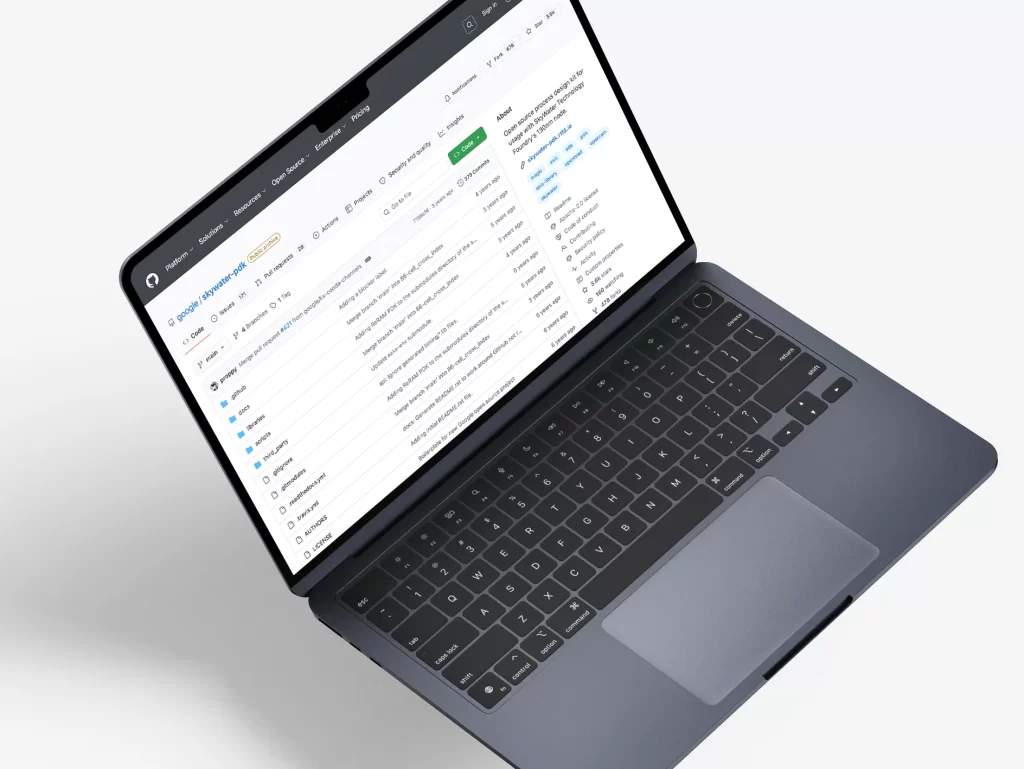
SkyWater has partnered with Google to create the first open-source process design kit, called SKY130, based on our 130nm CMOS platform.
Open source SKY130 PDK on Github
Github hosts the SKY130 Open Source PDK. There you can find key information, links to resources needed to get started quickly, and support. The SKY130 PDK is supported by a dedicated and talented group who are equally excited by the opportunity of making chip development available to everyone.

BUILD YOUR DESIGN ON PROVEN CMOS
Whether you’re developing a mixed-signal ASIC, integrating advanced sensing capabilities, or creating an entirely new technology platform, SkyWater provides the manufacturing expertise and collaborative engineering support to bring it to market.