By Thomas Sonderman, president and CEO, SkyWater Technology
A dynamic world drives our industry. As the world’s needs change, our industry changes right along with it. The semiconductor industry is now at an inflection point. To keep up with the needs of our changing world we must adapt to fully support technologies of the future such as quantum computing, hierarchical AI and high-speed communications.
As transistor node shrinking has slowed, technology leadership is now defined over a broad range of capabilities beyond just the smallest geometries. This growing diversity of devices in new dimensions of innovation creates a need for custom process development and business services.

When There’s No Moore Left
A considerable amount of time and effort has been invested in chasing Moore’s Law. It’s been a huge success that has left its mark on an industry that has adopted a fabless/foundry model. But as we continue to innovate to smaller geometries, we must also acknowledge that Moore’s Law via transistor scaling will come to an end. All indications are that silicon physics will prevent the industry from going beyond another two or three nodes. In addition to physical limitations, the aggressive drive toward silicon scaling has become cost-prohibitive for many applications.
This means that by sometime in the later part of this decade, the fabless/foundry model that has evolved to enable next generation products by shrinking geometries is going to have to create a new approach to delivering innovation the market demands. It’s going to be up to us in the industry to disrupt conventional thinking so we can begin preparing for life beyond the traditional manufacturing approaches we’ve relied on for so many years.
For the foundry segment to continue delivering manufacturing innovation, we’re going to have to embrace new materials, new architectures, heterogeneous integration, and new ways of enabling capability beyond traditional scaling.
“A foolish consistency is the hobgoblin of little minds.”
This famous quote by Ralph Waldo Emmerson points to the fact that the world is always changing and that being open to new thinking is the only way to meet future challenges and turn them in to opportunities.
Two of the biggest challenges facing our industry at the leading edge are memory bottlenecks and power wall constraints. Under Moore’s Law, memory bottlenecks are resolved by traditional methods of optimizing cache and memory usage, adding more physical memory, monitoring applications and drivers, stopping unused services, and of course, adding and developing faster chips. Power management involves multiple requirements for peak operation as well. We can optimize the design for better conversion efficiency, smaller size, improved heat dissipation – even allow dynamic voltage scaling – but I believe that for many applications there is a better model to tackle these challenges.
Our industry is built around innovation and thinking differently. The thinking that is required now should be about how to bring technology to market in a way that leverages the foundation that’s been created, but also embraces concepts that have been overlooked, ignored or previously lacked maturity to be considered.
A prime example of this thinking is carbon nanotubes. The industry has been talking about CNTs for the last 20 years, yet they’re not widely used. Other examples are superconducting and quantum computing – technologies with huge potential to help solve complex problems much faster than we can today. It’s time to take these novel and innovative ideas and bring them to the mainstream. But how do we do that?
What’s Old is New Again
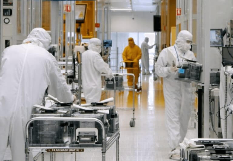
The industry is coming up against challenges that will require fresh thinking and innovative business models. But in a sense, we are going back to the past. There is a history in our industry of manufacturing-minded development which occurs in the same facility where manufacturing is scaled. But that’s going back to a time that 200 mm fabs drove the industry. These facilities operate in a sweet spot of automation that can support unconventional thinking without the constraints of a totally automated 300 mm fab. In many respects, we’re entering a golden age for 200 mm manufacturing. We’re seeing extraordinary utilization in these facilities globally as the market recognizes the unique value they provide to a very significant portion of the market.
A Better World
Technology for technology’s sake is a waste of money. The point of all this technology we’re creating is to make the world a better place. The compute paradigms we currently employ have been either enabled or supported by manufacturing innovation: transistor scaling, robust EDA infrastructure, substrate size increases and low-power device architecture.
These are the innovations that make cars safer, enable modern day cloud computing, are revolutionizing medicine and trade, and are changing the human experience with things like the ability to video call friends and family from nearly anywhere in the world.
But what’s next? In our view, it’s the adoption of the Technology as a Service℠ model into microelectronics manufacturing.
Technology as a Service
To support innovative thinking and new solutions, it’s important for product designers to be able to inject themselves into the product development process – from concept to productized solution – where they can make the most impact.
The thinking behind the Technology as a Service model is much like the thinking behind the Software as a Service model that has optimized the way software is brought to market.
With TaaS℠ you’re beginning the foundry engagement at earlier technology readiness levels than have become the norm in the industry. It’s about co-creating differentiated solutions in an agile environment where engineering teams can work with design teams to create an optimal end-state solution – a product that delivers differentiated value, but that is also highly manufacturable.
This is possible because there is a focus on design for manufacturability from the start. But it’s more than that. It’s design enabled manufacturing. The TaaS model places an emphasis on doing whatever is possible from a robust manufacturing perspective to enable out of the box device ideas of our customers. When you get to volume production, the TaaS model helps produce the highest possible yields, predictable cycle times, and very robust quality and reliability. This model also significantly accelerates time to market because early stage development is more efficient in a production environment, where the product can immediately scale to production since no transfer is required.
Stay tuned for Part 2 of this blog next week when we’ll dig further into the details of TaaS and how I believe this business model will drive the semiconductor industry well into the future.
About SkyWater
SkyWater is the only U.S.-owned and U.S.-based pure play semiconductor foundry and is a DOD-accredited Trusted supplier, specializing in custom technology development services, volume manufacturing and advanced packaging services. Through its Technology Foundry model, SkyWater’s world-class operations in Bloomington, Minnesota and Kissimmee, Florida provide unique processing capabilities to enable quality production and advanced packaging for mixed-signal CMOS, power, rad-hard and ROIC solutions. SkyWater’s Advanced Technology Services empower development of superconducting and 3D ICs, along with carbon nanotube, photonic and MEMS devices. The company serves customers in growing markets such as aerospace & defense, automotive, biomedical, cloud & computing, consumer, industrial and IoT. Please visit www.skywatertechnology.com/for more information.
For more information about SkyWater’s TaaS offerings, contact us and a member of our team will be in touch.
You can also watch our What is a Technology Foundry video here: https://www.skywatertechnology.com/about/